In this letter, we present fabrications and device characteristics of InGaAs p-i-n photodiodes, in which semiconductor microlenses are integrated by the diffusion-limited wet etching process. Also, the experimental data are compared with the results of numerical simulations and calculations.
Previously, three-dimensional (3D) topography simulators with moving boundary conditions have been developed to resolve exclusively the diffusion-limited etching problems. In these approaches, rigorous definitions of computational parameters and complicated calculation formalisms are required to simulate the bulge-shaped etch profile near the mask edge. In the case of microlens fabrication, however, our primary concern is the profile in the central region remote from the mask edge. The approach outlined below offers much simpler simulation formalism, while the results satisfactorily describe the surface profile of microlens around the lens center.
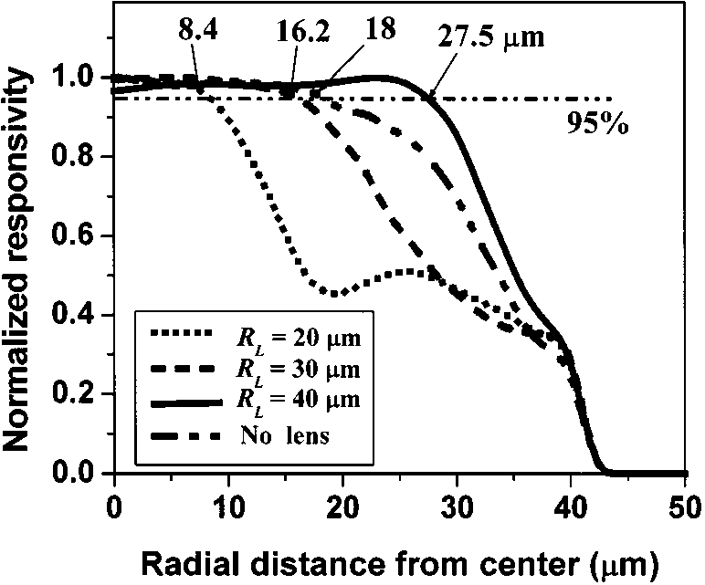
We measure the coupling tolerance for our microlensed PDs with lens diameters of 40, 60, and 80 m. Fig. 4 depicts the arrangement for fiber coupling measurement. A single-mode laser beam from a 1.55- m distributed-feedback (DFB) laser diode is launched into a single-mode fiber (SMF), and the exit fiber tip is then scanned around on top of a microlensed PD. Used in this experiment is a SMF, whose mode field diameter and radiation angle are known to be 9.3 m and 5 , respectively. The coupling efficiency as a function of the distance from the center is measured for each device, and the results are summarized in Fig. 5.

Fig1
We have successfully integrated InP microlenses on the backside of 1.55- m InGaAs PDs, using a single step diffusion-limited wet etching technique developed by ourselves. The microlens surface profiles are numerically simulated based on a simple diffusion theory, of which results agree very well with the measured data. Fiber coupling tolerance are also measured and compared with theoretical estimations using ray optics. The developed simulators help understand the microlens etch mechanism better, and also optimize further the microlens design to improve device performance for any given PD structure, beyond the measured 50% increase in fiber coupling tolerance.
The best result is obtained with the microlens with the lens aperture diameter of 80 m, and the measured coupling tolerance is 27.5 m. Here, the coupling tolerance is defined as the radial distance from the center to the point where the optical power detected by the PD drops to 95% of its maximum value at the center. The measured tolerance 27.5 m is well contrasted to 18 m for a PD without a microlens, which indicates over 50% increase in tolerance by the integration of a microlens. Smaller tolerances obtained for the other microlenses are attributed to the fact that a substantial portion of the tail of the impinging laser beam overlaps with the PD circumference where the lens profile has a curvature opposite to that of the central region, deteriorating the overall coupling efficiency.
上一篇: 湿法蚀刻制造的半导体微透镜