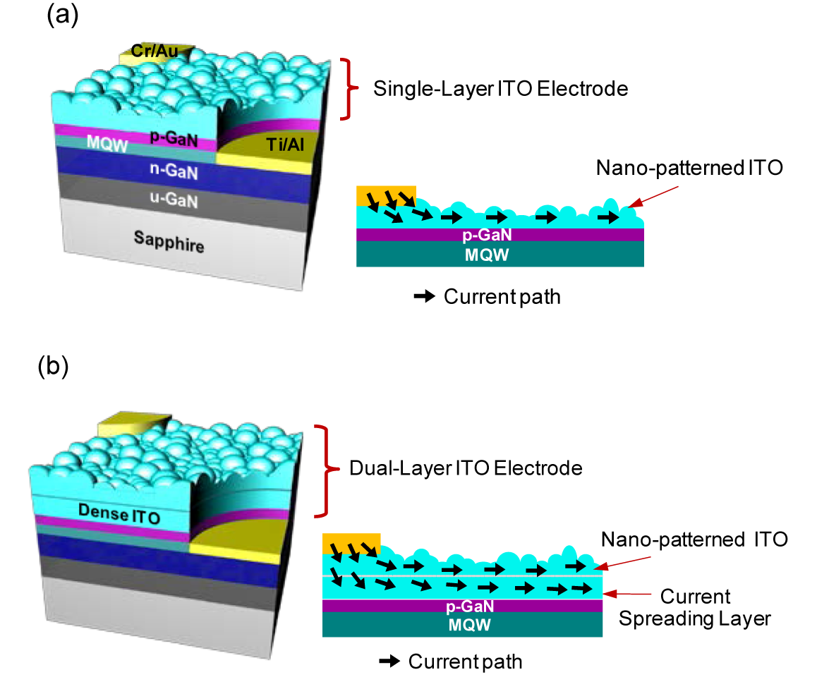
Abstract: We propose a dual-layer transparent Indium Tin Oxide (ITO) top electrode scheme and demonstrate the enhancement of the optical output power of GaN-based light emitting diodes (LEDs). The proposed dual-layer structure is composed of a layer with randomly distributed sphere-like nano-patterns obtained solely by a maskless wet etching process and a preannealed bottom layer to maintain current spreading of the electrode. It was observed that the surface morphologies and optoelectronic properties are dependent on etching duration. This electrode significantly improves the optical output power of GaN-based LEDs with an enhancement factor of 2.18 at 100 mA without degradation in electrical property when compared to a reference LED.
One of the most important issues in advancing solid-state lighting is to improve the light extraction efficiency of GaN-based light-emitting diodes (LEDs). Photons emitted from LED devices tend to be trapped within LED chips by the total internal reflection (TIR) at the interface between the indium tin oxide (ITO) transparent electrode and air/resin, which leads to a low light extraction efficiency [1]. The TIR at this interface can be effectively decreased by creating nano-scale patterns on the ITO electrode surface that have pattern dimensions smaller than the wavelengths of emitting light to allow more light emission out of the LED. Many ITO surface nano-patterning techniques, such as fabrication of photonic crystals [2,3], growth of nanowires [4], and surface texturing by photolithography or nano-imprinting [5–8], have been adopted to date, with apparent enhancement of light extraction efficiency [9,10]. However, current ITO nano-patterning methods either require expensive and time-consuming processes (such as photolithography and nano-imprinting) or involve harsh processing environments (such as high-temperature growth of nanowires or dry plasma etching). As a result, the underlying thin film components in the LED are quite often damaged after nanopatterning, and the overall device efficiency is therefore decreased.
atterning, and the overall device efficiency is therefore decreased. Recently, a simple maskless wet dip-etching technique for surface nano-patterning was introduced [11,12]. The LED with an as-deposited (before annealing) ITO layer was dipped into an etching solution for less than 10 seconds at room temperature. The short etching time and the room temperature process caused virtually no damage to other material layers of the LED. As compared to LEDs with a smooth ITO surface (referred to as “reference LEDs”), LEDs with ITO surfaces patterned with this method demonstrated a significant 30% increase in output light efficiency [10]. Although this low-cost process is promising for batch production of such highly efficient LEDs, several problems persist. First, the dip-etching time to obtain such a nano-patterned ITO surface is too short (<10 seconds) to make the process controllable. Second, after etching, the effective thickness of ITO for electronic conduction is decreased, which results in a significant increase in both the sheet resistance of ITO and the operating voltage of the LED, and consequently the device efficiency is sacrificed.

Fig1
The SEM images of etched surface morphologies are shown in Fig. 2. For SL400 and DL400/400, the patterns were uniformly distributed for etching times of 20 and 40 seconds, while the size and inter-distance of patterns increased and became rather random as etching time increased. For SL400 and DL400/400, the morphology evolutions with etching time were very similar, as expected, considering the same initial thickness of the etched ITO layer (400 nm). For SL800, the morphology evolution was also similar to those of SL400 and DL400/400, except that after 60 seconds, fine nano-bumps were still visible at the bottom of the surface, possibly due to the thicker initial ITO layer.