The im portance o f clean substrates in the fabrication o f microelectronic devices has been recognized since the dawn of semiconductor technology. Over the years, more com plex devices o f higher capacity have driven the industry to sm aller critical dim ensions and larger die sizes. In order to ensure device reliability, the scaling has necessitated stringent control o f defects in fabricated devices. The 4 gigabit technology node projected for first production ten years hence, requires that defect densities be restricted to less than 0.01 cm '2.1’ The removal o f defect causing microcontamination such as organics, particles and metals from the surface, is thus critical to achieving high yield, and its im portance cannot be emphasized enough.
Organic vapors from lubricants and greases serve as sources for organic contamination, and are often present on the wafers after grinding, lapping and polishing operations on w afers. Organic films deposited on exposure to room air or storage in plastic containers, along with photoresist and organic solvent residues also fall into this category. Layers o f such m olecular impurities are held in contact with the substrate surface by w eak electrostatic forces. Organic contaminants deposited on silicon wafers, may cause poIarizationJ and ionic drift due to the transport o f protons. 4 especially on surface sensitive M OS structures. Contam inant films on w afer surfaces can mask effective cleaning and rinsing, cause poor adhesion o f deposited layers, and lead to harmful decom position products. For example, when heated to a high temperature in an inert am bient, organic films can carbonize and form silicon carbide that can nucleate polycrystalline locations in an epitaxial deposit.
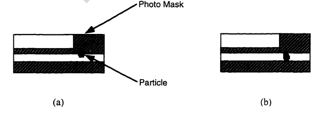
Some o f the defects arising from the interference o f particles with a photom ask pattern are best illustrated in Figure 1.2. Figure 1.2(a) shows a particle located on the border o f an opaque and a transparent region on a mask. If the transparent region corresponds to a metal pattern (negative photoresist), a large enough particle may cause local constriction o f the metal line, resulting in possible failure via electrom igration. 10 A situation such as the one shown in Figure 1.2 (b) could prove catastrophic, if the particle size is large enough so that the two opaque regions (on the mask) are connected. In the case o f a positive photoresist, a short between two metal lines could result: for a negative photoresist, the resulting defect could be a break in a metal line.
Particulate contam ination assum es significance in epitaxial grow th too. Its presence can degrade the quality o f epitaxial layers by interfering with the grow th o f films. It is suspected that the presence o f microscopic particles on the substrate, interferes with the ability o f the silicon atoms to follow the appropriate crystalline structure, during deposition from the vapor phase, in an epitaxial process. This in turn could result in crystalline defects, such as stacking faults. 11 Finally, particles can also severely impact gate oxide integrity, by influencing the rate o f oxide growth, resulting in a variation in oxide thickness across the surface.

Fig1
Metals are another m ajor source o f contam ination w hich lead to a reduction in yields and a degradation o f device parameters. The interactions o f metals with devices is much more subtle than that o f particles, so that they pose an even bigger challenge to the process engineer. Factors, such as the timings, temperatures and am bients employed in processing sequences, as well as the electrical field distributions, device size, and the presence o f structural defects and interfaces. 1 1 3 com plicate matters even further. 14 In other words, the extent o f the interaction varies significantly with the details o f the technology, so that m aking a generalization regarding an “acceptable" level o f contamination becomes difficult.
A com m on source o f metal contam ination is the hydrogen peroxide and/or ammonium hydroxide used in the pre-gate oxidation surface preparation step. If ultrapure forms o f these chem icals are used, bulk delivery systems become the bottleneck to reduction o f metallic im purities on the wafer surface. In addition. RIE systems and ionim planters in the fabrication facility often serve as sources o f the observed contamination.
上一篇: 氢氧化钾中硼硅酸盐玻璃的激光辅助蚀刻