Abstract: Large-scale high quality microlens arrays (MLAs) play an important role in enhancing the imaging quality of CCD and CMOS as well as the light extraction efficiency of LEDs and OLEDs. To meet the requirement in MLAs’ wide application areas, a rapid fabrication method to fabricate large-scale MLAs with high quality, high fill factor and high uniformity is needed, especially on the glass substrate. In this paper, we present a simple and cost-efficient approach to the development of both concave and convex large-scale microlens arrays (MLAs) by using femtosecond laser wet etching method and replication technique. A largescale high quality square-shaped microlens array with 512 × 512 units was fabricated.The unit size is 20 × 20 μm2 on the whole scale of 1 × 1 cm2 . Its perfect uniformity and optical performance are demonstrated.
Microlens arrays (MLAs) are crucial optical devices because of its broad applications in micro-optical systems, optical fiber coupling, artificial compound eye structures, light diffusers and optical sensing technology . However, the scale of MLAs remains a big obstacle, which restricts its further practical applications. Large-scale MLAs play an irreplaceable role in high resolution imaging and enhancement of light extraction efficiency of light emitting diodes (LEDs) and organic light-emitting diodes (OLEDs) . Notably, most of the image sensors are packed with square unit cells. In order to match with them, the MLAs should be fabricated square-shaped with high fill factor. Image sensors used in the high definition imaging field nowadays, like charge-coupled device (CCD) and complementary metal oxide semiconductor (CMOS), can hardly achieve a 100% pixel aperture ratios. The square-shaped MLAs can help to improve the ratio by focusing light on the photosensitive areas . That will enhance the CCD and CMOS devices’ signal to noise ratio (SNR), and improve its imaging capability. Furthermore, MLAs help to lower image sensors’ sensitivity threshold, achieving the approximate imaging effect of starlight CCD by using ordinary CCD. In solid state light market, low light out-coupling efficiency restricts the wide application of OLEDs and LEDs. In order to improve the output efficiency, microlens array is combined with OLEDs and LEDs. The output power of OLEDs and LEDs covered with microlens array could be enhanced by 2 times .
In this paper, we present a femtosecond laser wet etching technique , to fabricate high quality large-scale concave MLAs on glass. By improving the crafts and parameters, we solve the problems of efficiency, uniformity and quality. A large-scale concave MLAs with more than 260,000 units was fabricated.
Theoretically, the fabrication procedure of the large-scale square-shaped MLAs is basically the same with the small-scale ones. However, in the actual fabrication process there are some factors, including the flatness of the sample, continuous operation ability of the mechanical shutter and the irradiance uniformity of fs-laser and so on, which restrict the feasibility to fabricate large-scale MLAs. Therefore, the crafts and parameters are improved to fabricate it. The optimizational crafts and parameters will be discussed in Section 4.
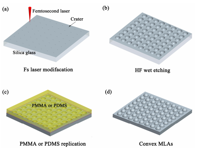
Here we show the process of fabricating MLAs by fs-laser wet etching method. As shown in Fig. 1, the fabrication process can be divided into a four-step process, including fs-laser exposure, wet etching, replica molding and cleaning . Firstly, fs-laser pulses (800 nm, 50 fs, 1 KHz) with laser power (P) of 5mW were focused onto the surface of silica glass by an objective lens (NA = 0.5), generating a square-arranged laser-modified spots array [Fig. 1(a)]. The laser exposure craters were generated point-by-point. For each point, the exposure time could be controlled by a fast mechanical shutter and the laser power could be tuned through a variable density filter. Subsequently, the post-preparative sample was treated with 3% hydrofluoric (HF) acid solution at room temperature. The square-arranged craters were transformed into square-shaped concave structures after the wet etching process [Fig. 1(b)]. During the etching process, it is worth to point out that an ultrasonic bath is used to guarantee the conformity of the microlenses and high speed of the etching process. The ultrasonic bath is conductive to removing the products and bubbles produced during the etching process. Then, the convex MLAs could be replicated by pouring liquid PDMS onto the square-shaped concave structures and keeping it at the temperature of 80 °C for about 60 minutes [Fig. 1(c)]. Finally, we could get square-shaped convex MLAs on the surface of solidified PDMS by removing the mold [Fig. 1(d)]. Additionally, owing to thermoplastic effect of PMMA, convex MLAs could be also fabricated by pressing PMMA chip onto the mold at the temperature of 120 °C for several minutes.

Fig1
Figures 3(a) and 3(b) show the SEM images of the square-shaped MLAs captured from different angles and different magnifications, which excellently reveal the MLAs’ perfect surface quality and uniformity. Figures 3(c) and 3(d) present the three-dimensional (3D) morphologies and cross-sectional profiles of the concave structures which were observed by a CLSM. The inserted figure in Fig. 3(d) shows the SEM cross-sectional profiles of the concave structures. The side length of the square-shaped concave microlens is 19.967 μm, which is very close to the interspaces (20 μm) that we set at the beginning, and the depth of the microlens is 2.352 μm. The curvature radius, R, of the square-shaped concave MLAs can be figured out by a simple equation: R = (h2 + r2 )/2h (1), where h is the depth of the microlens, r is a half of the side length of the squared-shaped microlens. After the calculation, the result of the curvature radius of the concave microlens is 43.56 μm. The focal length of the microlens array, f, can be calculated by the equation: f = R/(n-1) (2), where n is the value of the refractive index of the silica glass at wavelength of 633 nm. Considering the approximation of n, 1.45, the focal length of microlens array equals 96.8 μm.
上一篇: Pre-Gate氧化清洗顺序的优化
下一篇: 基板预栅极清洗的系统和方法