A System and method for cleaning Semiconductor wafers wherein the use of SCI and SC2 is eliminated and replaced by the use DIO and dilute chemistries. In one aspect, the invention is a method comprising: (a) Supporting in a process chamber at least one Semiconductor wafer having a Silicon foundation with a silicon-dioxide layer in at least one pre-gate structure; (b) applying an aqueous Solution of hydrofluoric acid in deionized (DI) water to the semicon ductor wafer to remove the Silicon dioxide layer and form a gate; (c) applying OZonated deionized water (DIO) to the Semiconductor wafer to remove particles from the gate and passivate the Silicon foundation; (d) applying a dilute Solu tion of hydrofluoric acid and hydrochloric acid in DI water to the Semiconductor wafer to remove any Silicon dioxide layer that may have formed in the gate from the application of the DIO and to remove any metal contaminants, and (e) applying DIO to the Semiconductor wafer to grow a new layer of Silicon dioxide on the Silicon foundation in the gate.
Conventionally in semiconductor manufacturing, wet cleaning of Semiconductor uses the Sequential chemical recipe of hydrofluoric acid (“HF"), Standard Clean 1 (“SC1'), and Standard Clean 2 (“SC2') for pre-gate clean ing, which is referred to as the Shorthand Sequence HF--SC1+SC2. This cleaning sequence is designed to remove bulk silicon dioxide (“SiO”) by HF, followed by cleaning particles with SC1 (which is mixture of deionized (“DI”) water, ammonia hydroxide (“NHOH'), and hydro gen peroxide (“HO)), and then to clean metals with SC2 (which is a mixture of DI water, hydrochloric acid (“HCl") and H2O). This sequential cleaning process is then typically followed by a final isopropyl alcohol (“IPA”) drying step. An intermediate DI water rinsing usually takes place between each step. It is important to clean the silicon (“Si”) Surface of the semiconductor Substrates after the HF and before the SC1 re-grows an SiO layer. Any defects attrib uted to particles, metals or Surface roughness in the Si-SiO, interface could cause the electric testing of oxide charge to-breakdown (Q) failure, resulting in device yield reduc tion.
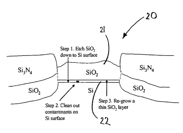
The allowance of defects becomes very stringent as device size shrinkS. Thus, the pre-gate clean becomes increasingly critical as it directly impacts the interface. A pre-gate cleaning recipe is typically required to accomplish three steps in the following order: (1) remove the top SiO, layer, typically in the range of 130 A; (2) clean particulate and metallic contamination on the Si Surface once the SiO2 layer is removed with the creation of minimum Surface roughness; and (3) re-grow a thin SiO2 layer for the gate SiO, after the particulate and metallic contamination is cleaned from the Si Surface.

Fig1
These and other objects are met by the present invention. In Some embodiments, the System and method of the present invention utilizes a modification of the tradi tional Sequential pre-gate cleaning recipe of HF-SC1+SC2 by using DIO to replace the SC1 and/or using DIO to re-grow the SiO layer. In one embodiment, the modified recipe of the present invention comprises HF--DIO+dHF/ HCl-DIO, wherein dHF/HCl stands for an diluted aqueous Solution of HF and HCl. The use of this modified revision reduces Si Surface damage and re-grows a high quality SiO2 layer, without Significantly reducing particulate and metallic removal. When used in conjunction with the pre-gate clean ing of 0.15 um flash memory devices, the modified pre-gate cleaning recipe has shown to improve the yield of the production.
下一篇: 过渡金属二硫属化物单层的反应等离子体清洗