The effects of wafer spin speed during a wet cleaning process after dry etching of a metal line patterning was investigated in detail. In this experiment, a conventional single wafer spin tool was used to clean 200 mm wafers with a dilute acid mixture (sulfuric acid; H2SO4 5.5 wt% and hydroflfluoric acid; HF 0.01 wt%) in de-ionized water (DIW). We confifirmed that the polymer removability, the pitting, and the electrical resistance of a metal line were dependent on the wafer spin speed. Moreover, very different results were obtained from the center and edges of the wafer. When the dilute acid mixture is supplied onto the wafer center, the chemical is consumed with a chemical reaction toward the wafer edge. When large size wafers are used, or the wafer spin speed is lower, more degraded chemical could be transported to the wafer edge. A higher spin speed is useful for wafers of large size (300–450 mm) as an effective parameter in the cleaning process based on this experiment result.
Various contaminants are present during device processes in a real production line in ultra large scale integration (ULSI) fabrication. Since a very clean surface is required on ULSI device processes, the contamination must be removed by cleaning techniques, such as wet cleaning using a batch-dip tool, a batch-spin-spray tool , or a single-wafer-spin tool. In the batch-dip tool, there is a concern about cross-contamination which is caused by the transfer of particles in between wafers in a sink compared to the other wet process tools. Batch-spin-spray tool is used to perform postetch interconnect cleans in back end of line (BEOL) . The batch-spin-spray tool gives much more advantage for the cost effectiveness in a high volume production line when dilute-acid chemicals (mixtures of H2SO4, H2O2, and HF with de-ionized water (DIW)) are used .
An 800 nm thick plasma chemical vapor deposition (CVD) SiO fifilm (SiO2 fifilm) was deposited using SiH4 and N2O as an underlying layer on bare Si wafers. Metal fifilms consisting of 20 nm Ti, 50 nm TiN, 400 nm AlCu (Cu 0.5%), and 0.7 nm TiN were deposited on the SiO2 fifilm. A metal line pattern was then created using a photo mask (resist thickness 1500 nm) dry etching with BCl3 and Cl2 (in Lam research TCP9600PTX, with O2 plasma inline-ashing). The length, width, height, and spacing of the metal line patterns were 4.5, 1.2 (or 0.35), 0.5, and 1.0 (or 0.5) lm, respectively. The samples were inspected for wafer defects using a KLA2139 and a scanning electron microscopy (SEM).
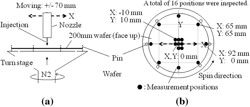
In this experiment, a conventional single-wafer-spin tool was used (Fig. 1a and b). Wafers were placed on the turn stage, and then the wafers were raised with N2 in order to avoid contact with the turn stage. After the chemical was dispensed from the injection nozzle, the wafers were rinsed and dried using DIW and a spin-off with N2, respectively (Fig. 1a). During the wafer processing, a total of 6 pins grip the wafer edges (Fig. 1b). In this experiment, the nozzle moving distance was selected as ±70 mm (on X axis) from the wafer center position (X,Y = 0,0 mm) as shown in Fig. 1a. Inspection locations within the wafer are shown in Fig. 1b. A total of 16 positions within wafer (8 positions each at the center and edges of the wafer) were inspected.

Fig1
Fig. 3a shows a wafer defect map after cleaning the wafer using condition #1. The defects were recognized at the wafer center. The pattern peeling as well as the side etching of the metal line was observed at the defect area located at the wafer center (Fig. 3b). Based on above result (Fig. 2a) and the reports [5,7,8], the pattern peeling at the wafer center could have happened by the vertical chemical injection (Fig. 3b). We assume that the polymer removal ability, the pitting generation, and the pattern peeling on the metal line are closely related to the wafer position, which induces different chemical flflows.
We next determined if the electrical resistance of the metal line was altered by the cleaning conditions, since the wafer spin speed impacted polymer residue (Fig. 2b) and the generation of pits (Figs. 2a, 3) on the metal. Fig. 5a shows the metal line resistance (cumulative probability of the metal line resistance) using the cleaning condition of #3 shown in Table 1. We found that the metal line resistance at the wafer edge was lower than that at the wafer center. Therefore, we hypothesize that the metal line resistance at the wafer center was increased by the enhanced side etching of the metal line due to the higher chemical flflow. Fig. 5b shows the relationship between the wafer spin speed and metal line resistance under the cleaning conditions #1–5 in Table 1. The metal line resistance at the wafer center was higher than that at the wafer edge under these conditions. However, the disparities in the metal line resistance within the wafer decreased as the wafer spin increased. The higher spin speed could have slightly increased the resistance at the wafer edge with the enhanced side etching of the metal line, in contrast to the decreased resistance at the wafer center with the reduced side etching of the metal line. This fifinding is also supported by the relationship between the wafer spin speed and the generation of pits (Fig. 4). We also measured the metal line resistance during chemical treatment using a moving nozzle. A moving nozzle worked well for reducing the variation to within 3% using a spin speed of 400 rpm.
上一篇: 醇碱溶液中多孔硅的化学氧化
下一篇: 去除碳化硅衬底中的表面污染物