Wide bandgap semiconductors are becoming the new platform of choice for devices with greater power density and higher energy efficiency than silicon. In particular, Silicon carbide (SiC) is ideal for high power and high temperature (>150 ºC) electronic applications because of its excellent properties as a high critical electric field for operate under high applied operating voltages (2500 kV/cm) and good thermal conductivity (4.9 W/cmK) [1]. However, heteroepitaxial film growth of functional oxides on SiC, is a challenging and yet critical goal to achieve the overall success of utilizing SiC in next-generation electronics. Formation of an abrupt and effective interface is one of the basic requirements for integration of functional oxides on semiconductors. A reliable and successful cleaning procedure must be developed in order to produce consistent and well-characterized starting surfaces. Several SiC surface cleaning studies, including high-temperature hydrogen etching and hydrogen plasma treatment, have been reported to remove contaminations and scratches made during polishing.
In our previous work, 6H-SiC (a polymorph of SiC with the hexagonal structure) substrates were cleaned in an ex-situ hydrogen (H2) furnace [3]. A tantalum foil strip placed under the sample is used as a heating element during furnace operation. X-ray photoelectron spectroscopy (XPS) scans of resulting 6HSiC surfaces repeatedly show 10 at% oxygen contamination on the surface. This aspect, along with the sharp non-diffusive spots known as intermediate Laue rings observed in the reflection high energy electron diffraction (RHEED) pattern, confirm the √3×√3 R30° surface reconstruction which corresponds to the presence of a silicate adlayer on the surface. These results are consistent with previous reports for cleaning of SiC [2]. However, the high treatment temperature (~1600 ºC) and high sensitivity to small thermal gradients makes this process impractical for low-cost, high-throughput production.
In this current study, hydrogen atoms to be used for cleaning, are produced by dissociation of hydrogen gas at the hot surface of a hydrogen atom beam source (HABS). The HABS is a thermal gascracker cell consisting of a tungsten filament set in high purity tungsten tube. 6H-SiC substrates were degreased with organic solvents and then introduced into UHV (ultra-high vacuum) chamber. Then they were exposed to hydrogen (H) atoms with flux of 4.5×10+14 atoms/cm2 .sec at substrate temperature of 700 ºC. All subsequent surface analysis were carried out in situ without breaking vacuum.
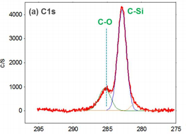
The XPS scans of atomic hydrogen-cleaned 6H-SiC surface reveal the presence of 8 at% oxygen on the surface, below the value of 10 at% oxygen that was achieved via use of an ex-situ hydrogen (H2) flow furnace. The chemical bonding states of silicon (Si 2p spectrum) as shown in Figure 1(d) illustrates the removal of Si-O bond from the surface after atomic hydrogen (H) cleaning. In addition, as seen in Figure 1 (a, c), the C-O bond signal decreased in magnitude, but does not disappear completely after cleaning. These results suggest that all remaining oxygen on the surface bond to carbon but not to silicon. Further, RHEED data do not show the anticipated reconstructed √3×√3R30º structure as the intermediate Laue rings are not observed (Figure 1(f)). This result is likely due to absence of a silicate adlayer on the surface.

Fig1
Overall, these results indicate that the treatment of 6H-SiC surfaces using an atomic hydrogen (H) beam source and using a hydrogen (H2) flow furnace will produce surfaces with different chemistries as well as different structures. Atomic hydrogen certainly reduced amounts of oxides on the surface at a comparatively low temperature. Further investigation is required to better understand the reactions between hydrogen and carbon on the surface. The successful surface preparation to produce a clean and smooth starting surface can open new possibilities for heteroepitaxy of many two-dimensional electronic materials.
上一篇: 湿清洗后晶圆旋转速度对金属线的影响
下一篇: n型多孔硅刻蚀时间的效应