Porous silicon layers have been prepared from n-type silicon wafers of (100) orientation. SEM, FTIR and PL have been used to characterize the morphological and optical properties of porous silicon. The inflfluence of varying etching time in the anodizing solution, on structural and optical properties of porous silicon has been investigated. It is observed that pore size increases with etching time and attain maximum for 20 minutes and then decreases. The PL spectrum peak shifts towards the higher energy side, which supports the quantum confifinement effect in porous silicon. The FTIR shows that the Si-Hn peaks are observed at the surface of the PS layer and these chemical species also give raise the PL in PS.
Silicon has historically been the dominant material for electronics, while work in optoelectronics has relied almost entirely on III – V compound materials such as GaAs and InP. The primary reason for this dichotomy of materials systems has been the tenet that light emission from silicon is impractical because of its indirect band gap structure [1]. However the observation of room temperature visible photoluminescence1 (PL) in porous silicon has demonstrated the potential for practical, effificient silicon based emitters for optoelectronic applications [2,3]. As a result the porous silicon (PS) layers fabricated by electrochemical etching, followed by pore widening treatment to decrease the pore wall dimension, have become subjects for intensive investigation [1,4]. Porous Silicon can exhibit a large variety of morphologies and particle size. It has been reported that the luminescence of the PS is ascribed to the quantum confifinement effect (QCE) as well as to the presence of Si-Hn bond near the surface of nano crystallites. However the exact luminescence mechanisms and relevant nanostructures still remain unclear [5]. So intensive studies on PS continues.
By adjusting the formation parameters, porous silicon with large range of porosities and morphologies can be produced, which can be tuned for several applications. In all PS applications, information about the pore size and their distribution and surface chemistry and their dependence on the fabrication conditions plays a decisive role [6]. Correlation of observed physical properties with the morphology of PS fifilms and the relationship between PS morphology and preparation parameters is necessary. Principal parameters controlling macro pore formation depend on the properties of silicon substrate (crystal orientation, doping), anodizing solution and temperature [6]. For a given substrate at a fifixed temperature, the pore formation will be determined by the properties of anodizing solution (HF concentration, current density, etching time and bath illumination condition). In the present work, an attempt has been made to study the relationship linking the morphology, optical properties and fabrication conditions of porous silicon formed using n-type material.
Porous Silicon samples were prepared from n-type Silicon wafers (100) orientation with a resistivity of 50 Ω cm. The samples have been prepared by keeping the HF: ethanol ratio and current density constant at 1:2 and 30 mA/cm2 respectively and varying the etching time and during anodization the wafer was illuminated by a halogen lamp of 300 W. After anodization the porous silicon samples were rinsed in ethanol. The etching time used for the anodizing process has a strong inflfluence on the porous silicon properties [7]. So the etching time is to be varied to study its inflfluence on the PS characteristics. The experimental data on the relationship between the etching time and the morphological and the optical properties are discussed in the following sections.

Fig1
Thus the study shows that the pore size and hence the porosity of PS depends on the etching time i.e., the etching time is a parameter controlling the pore size hence the porosity of the PS. It can be further noted that even when the etching time is increased by 10 minutes beyond the etching time of 20 minutes which gives the maximum pore size, some of the pore walls alone break, exposing a small portion of the next layer; a further increase of 10 minutes in etching time (totally 40 minutes) is needed to break most of the thin pore walls and expose most part of the next layer. This can be interpreted to mean that the thin pore walls are strong. Such a conclusion is in excellent agreement with the report of Lehmann and Gosele [3] on the strength of the thin pore walls.
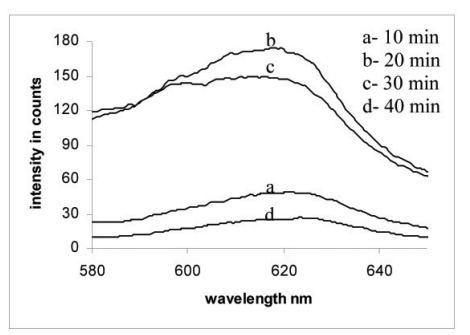
The photoluminescence (PL) spectra of the n-type porous silicon formed using different etching times of 10, 20, 30 and 40 minutes are displayed in fifigure 2. It can be seen that room temperature PL in the visible region has been obtained for all the etching times used. The PL intensity maximum has been found to occur at 624 nm and 619 nm for the etching times of 10 and 20 minutes respectively, indicating that there is a blue shift of the PL maximum with etching time.
上一篇: 去除碳化硅衬底中的表面污染物
下一篇: Si蚀刻:温度依赖性