In this paper, the method of space alternated phase shift (SAPS) megasonic technology is applied for post-etch (Bosch) TSV wafers cleaning process. The SAPS technology provides uniform sonic energy on each point of entire wafer by alternating phase of megasonic wave in the gap between a megasonic device and the wafer. For this study, 5x50 µm post-etch (Bosch) TSV wafers were used. Experimental verification is provided using both physical analysis and electrical test. SEM equipped with an EDX was used to detect the presence of fluoropolymer residue (i.e., CXFY) for pre- and post-cleaning TSV coupons, FIB-SEM was used to evaluate copper plating performance; TSV leakage current map and Voltage ramp dielectric breakdown (VRDB), which act as principal electrical reliability metric, were also used to assess cleans effectiveness. The test results indicate that the megasonic energy can propagate to the bottom of TSV, and the wafers undergo SAPS cleaning process exhibit obvious electrical performance enhancement comparing with those cleaned by conventional single-wafer spray approach.
The Bosch etch is a typical reactive ion etch (RIE) process that produces high aspect ratio (HAR) via TSVs (10:1 or 20:1 depth-to-diameter ratios). The RIE process used to fabricate TSVs requires rapidly alternating isotropic plasma etch and fluorocarbon polymer deposition steps, resulting in fluoropolymer etch residue on the sidewall of the vias. This residue has the potential— if not thoroughly removed from the sidewalls—to inhibit the growth of the dielectric liner, resulting in compromised isolation of the TSV and reduced device yield. Liner discontinuity and non-uniformity can also cause barrier layer delamination and increase thermal stress of the metal interconnects due to non-uniform sidewall profiles or copper voiding.
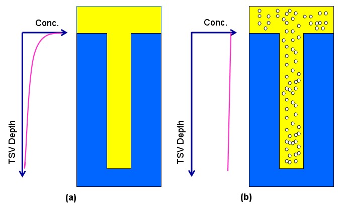
In this study, space alternated phase shift (SAPS) megasonic technology is applied to sidewall residue removal in post TSV etch cleaning. The SAPS technology provides uniform sonic energy to the wafer surface by alternating the phases of megasonic waves in the gap between the megasonic transducer and the wafer. Chemical radicals that remove residues are generated in dilute solution and promoted by megasonic energy. Furthermore, the mechanical force of bubble cavitation generated during the megasonic agitation enhances the mass transfer rate and improves residue removal efficiency during the cleaning process (Fig. 1). Compared to conventional wet clean methods, SAPS megasonic technology exhibits high residue removal efficiency and low material loss for high aspect ratio vias. Furthermore, it causes minimal damage to structures (1), (2).

Fig1
Experimental verification is provided using both electrical test and physical analysis. Results indicate that the megasonic energy can propagate to the bottom of TSV through cleaning solution. For this study, 20 5x50 μm post-etch (Bosch) TSV wafers were used for evaluating cleaning performance. Wafers were split into 2 groups: The 1st group consisted of wafers cleaned with conventional single-wafer spray cleaning, and the 2nd group was composed of wafers cleaned using SAPS megasonic cleaning technology. For experimental verification, the evaluation methodology included SEM equipped with an EDX to detect the presence of fluoropolymer residue (i.e., CXFY) for pre- and post-cleaning TSV coupons. FIB-SEM was used to evaluate copper plating performance.
In general, incomplete cleaning will have a deteriorating effect on device performance, particles and residue left in the TSV holes would result in a low breakdown voltage, a high leakage current, shifted threshold voltage and low yields. The SAPS clean recipe indicates lower overall leakage current at +5V compared to single-wafer cleans recipes (Fig. 2). Wafer maps and TSV leakage current distribution plots show consistently better performance with the SAPS clean recipe, with more die having leakage current levels below 1e-10 A in wafers that underwent SAPS (Fig. 3 a and b) compared to the conventional single-wafer clean process (Fig. 3 c and d). VRDB results showed that higher average breakdown voltage (Fig. 4 a) and lower average breakdown current (Fig. 4 b) occur with a SAPS cleaning process compared to a conventional single-wafer cleaning approach.
In this paper, a promising SAPS cleaning technology applied in post-etch (Bosch) TSV wafers is presented. From the experimental results, the SAPS technology provides uniform megasonic energy distribution to the wafer surface and has a significant capability for TSV residue removal. VRDB results show the TSV wafers undergo SAPS cleaning process exhibit obvious electrical performance enhancement comparing with those cleaned by conventional single-wafer sprayapproach.
下一篇: 高效光伏硅片制造中的水基超声化学清洗