Thermal behavior of 200-mm- and 300-mm-diameter Si (100) wafers during high-temperature rapid thermal processing (RTP) in a single wafer furnace (SWF) is investigated as a function of temperature, pressure, process time, wafer handling method and speed. Signifificant elastic wafer shape deformation was observed during wafer temperature ramp-up. Slip generation was frequently observed in wafers processed above 1050 C. Size, shape and spatial distribution of crystal defects generated during RTP were characterized using an optical microscope and X-ray topography. The wafer handling method and speed are found to be very important in reducing defect generation during RTP at the given process conditions. Highly reproducible, slip-free RTP results were achieved in 200-mm- and 300-mm-diameter Si (100) wafers processed at 1100 C by optimizing the wafer handling method and speed.
In semiconductor thermal processing applications, batch processing was adopted in the early stage in the industry and is still very popular. A typical batch furnace requires a 150– 200 wafer load per batch and very long cycle times (from wafer in to wafer out) ranging from 4 to 10 h per batch depending on the process time due to slow ramp-up ( 10 C/ min) and ramp-down (~3℃ C/min) rates.1,2) Batch furnaces are able to meet the requirements for many thermal processing applications, even for 0.18 m technology.
In addition to the device dimension and allowable thermal budget decrease, the need for improved ambience control due to the introduction of new materials requires a single wafer processing system.2,3) In terms of thermal budget reduction and process flflexibility improvement in operating temperature and lot size, fast ramp mini batch (5–25 wafer load per batch) processing or single wafer rapid thermal processing (RTP) technology has signifificant advantages over thermal processing in conventional batch furnaces.1–3) Typical cycle times in the mini batch furnaces and RTP systems are 1–2 h per batch and 1–5 min per wafer, respectively. The ramp-up and ramp-down rate ranges for the mini batch furnaces and the RTP systems are on the order of 10℃/s and 100℃/s. Rapid wafer temperature ramp-up and ramp-down make the thermal process very effiffifficient without increasing the thermal budget. However, a small temperature gradient on wafers heated above 1000℃ can cause plastic deformation (crystalline slips), which strongly affffects device yield.4,5) Slip-free high-temperature processing of large-diameter (200 mm and above) Si wafers in the fast ramp mini batch furnaces and single wafer RTP systems is diffiffifficult.
Large size (200 mm and 300 mm in diameter) Si (100) wafers were annealed in a preheated SWF process chamber in the temperature range of 800–1150 C. It is well known that the mechanical strength of Si wafers is strongly affffected by the impurity type and concentration. The inflfluence of oxygen and boron in Si on the mechanical strength has been studied and published in detail.7,8) In this experiment, Si wafers with low oxygen concentration were used as control samples. Crystalline defects generated in Si wafers during annealing are investigated by visual inspection and optical microscopy as a function of temperature, pressure, process time, wafer handling method and speed.

Fig1
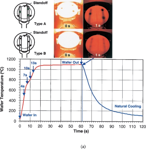
Time elapsed side views of the wafer in the process chamber at 1100 C as seen from the gate valve port during wafer temperature ramp-up are shown in Fig. 2(b). The photographs were taken 4, 7, 10 and 13 s after wafer insertion into the preheated process chamber. The wafer is placed on three quartz standoffffs located in the quartz process chamber. The dark hole in the center seen in side-view photographs is the process gas inlet. The wafer shape starts to deform as time passes (wafer temperature increases). A maximum vertical wafer deformation of 10 mm was observed 10 s from the wafer insertion. An average wafer temperature at 10 s from the wafer insertion is approximately 800 C. The wafer becomes flflat at 13 s ( 950 C) from the wafer insertion. Temperature nonuniformity within the wafer during rapid wafer temperature ramp up caused the elastic wafer shape deformation due to nonuniform thermal expansion. The wafer temperature becomes uniform in 13 s and the wafer shape becomes flflat again.