Microwave photonics uses light to carry and process microwave signals over a photonic link. However, light can instead be used as a stimulus to microwave devices that directly control microwave signals. Such optically controlled amplitude and phase-shift switches are investigated for use in reconfgurable microwave systems, but they sufer from large footprint, high optical power level required for switching, lack of scalability and complex integration requirements, restricting their implementation in practical microwave systems. Here, we report Monolithic Optically Reconfgurable Integrated Microwave Switches (MORIMSs) built on a CMOS compatible silicon photonic chip that addresses all of the stringent requirements. Our scalable micrometer-scale switches provide higher switching efciency and require optical power orders of magnitude lower than the state-of-the-art. Also, it opens a new research direction on silicon photonic platforms integrating microwave circuitry. This work has important implications in reconfgurable microwave and millimeter wave devices for future communication networks.
Te SOI wafer consists of 250nm-thick device layer and 3μm-thick buried oxide layer. During the fabrication process, most of the silicon material is removed to form Si photoconductive patches with dimension of 16 μm by 12 μm. Single-mode SiNx ridge waveguide with the dimensions of 800nm-width and 400nm-height are fabricated and used to guide light toward Si patches in order to activate them at diferent locations on the chip. Te ridge waveguide and Si photoconductive patch are cladded by 1µm-thick SiO2 layer. Te Ground-Signal-Ground (GSG) transmission lines consist of 800nm-thick Al lines with a tapered signal electrode toward the Si photoconductive patch.
Figure 1c,d show the SEM images of MORIMSs of both types. Te SiNx waveguide conformally covers the Si photoconductive patch without any crack and discontinuity. Tis process is CMOS compatible and the details of the nanofabrication are described in Method.
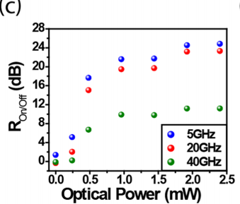
Te On/Of performances of the MORIMS are characterized by measurements of the S-parameters. Te experimental details are described in the Characterization section. Figure 2a,b show the measured S21 parameter of tapered- and through-type structures at On and Of state up to ~40GHz. In Fig. 2a there is a dip in S21. Tis is due to the imperfection of the transmission line. More precisely, the 21GHz frequency corresponds to free spectral range between the probe and the gap. Te fact that this frequency shifs slightly when the gap is illuminated testifes a change of the dielectric constant. To characterize the switches performance, the extinction ratio Ron/of n/|S21(On)/S21(Of)| is adopted as the fgure of merit that qualifes amplitude switching efciency for a given microwave frequency7 . Figure 2c,d show Ron/of with respect of input optical power at frequencies of 5GHz, 20GHz and 40GHz. Overall, the On/Of ratios increase linearly from 0 to ~1.5 mW before reaching a saturation plateau. As expected, the tapered-type switch shows higher performance, with switching efciency of ~25 dB and ~23 dB at 5GHz and 20GHz, respectively compared to ~14 dB and ~12 dB achieved at same frequencies with the through-type confguration. Although the through-type is less efcient under same incident optical power, the remaining energy in the waveguide can be used to control another switch as shown next. It is worth mentioning that the switching time of the proposed device is on the order of few micro-seconds which is compatible with beam steering and beamforming applications requirements.
Te proposed optically reconfgurable switches are a proof of concept that can be easily implemented in beamforming and beam steering microwave systems which require moderate switching time constant. Moreover, the proposed integrated devices could also enable more advance functionalities when combining other well-established photonic building blocks such as ring resonators, directional couplers and Mach-Zehnder modulators on the same chip (discussed in Supplementary Information Section IV). Te proposed approach can be tailored in the future generation of ultra-high frequency communications systems which will face stringent requirements in terms of frequency bandwidth, power consumption, size and packing density, and low-cost for mass production. In that area, ultra-fast photoconductive switches exploiting III-V materials, with ultra-short carrier lifetime, are required and outstanding eforts has been already made. Te proposed approach could be exploited in sampling application that requires the combination of several switches with very accurate time delays between them. Tis work is a real added value for developing integration technology for microwave signal processing. Besides, in our case, the microwave signal is optically processed but in the microwave domain directly, thus relaxing the constraint of up-converting the microwave signal to an optical carrier which leads to conversion losses and additive noise. Accordingly, the MORIMS architecture can be directly implemented in any microwave sub-system such tunable microwave flters of larger systems such as phased array antennas.

Fig2(c)
In summary, we have demonstrated monolithic optically reconfgurable integrated microwave switches on a SOI chip. Our approach consists of co-integration of microwave circuits with integrated photonic devices to form optically reconfgurable microwave switches. A single input SiNx waveguide is used to route the light toward switches at diferent location on chip. Integrated photonics provides miniaturized Si photoconductive patches, high confnement of light in the waveguide and high coupling efciency of light from waveguide to silicon photoconductive microwave switches. Consequently, the demonstrated engineered devices outperform their classical analogues in term of On/Of switching efciency, footprint and optical power level requirement. We experimentally demonstrate high microwave amplitude switching performances of over 25dB around 5GHz, 23dB around 20GHz and 11dB at 40GHz, and lower optical power requirement (~2mW) by orders of magnitude lower than the state-of-art photoconductive switches. Scalability is a challenge that has been also advanced by demonstrating integrated multiple reconfgurable switches on the same SOI chip with high amplitude switching performance. Moreover, phase shifs of 20° and 60° were measured for microwave signals at 20GHz and 40GHz, respectively. Tis work is an important step in introducing photonics into direct processing of microwave signals, paving the way towards optically reconfgurable microwave and millimeter wave devices for future ground, embedded radar systems, and emerging 5G wireless communication networks.
上一篇: 用硅光子纳米力学界面转换微波和电信光子
下一篇: 聚硅薄膜上的CMP后新型清洁解决方案