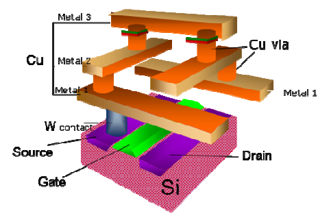
As multistep, multilayer processing in semiconductor industry becomes more complex, the role of cleaning solutions and etching chemistries are becoming important in enhancing yield and in reducing defects. This thesis demonstrates successful formulations that exhibit copper and tungsten compatibility, and are capable of Inter Layer Dielectric (ILD) cleaning and selective Ti etching.
The corrosion behavior of electrochemically deposited copper thin films in deareated and non-dearated cleaning solution containing hydrofluoric acid (HF) has been investigated. Potentiodynamic polarization experiments were carried out to determine active, active-passive, passive, and transpassive regions. Corrosion rates were calculated from tafel slopes. ICP-MS and potentiodynamic methods yielded comparable Cu dissolution rates. Interestingly, the presence of hydrogen peroxide in the cleaning solution led to more than an order of magnitude suppression of copper dissolution rate. We ascribe this phenomenon to the formation of interfacial CuO which dissolves at slower rate in dilute HF. A kinetic scheme involving cathodic reduction of oxygen and anodic oxidation of Cu0 and Cu+1 is proposed. It was determined that the reaction order kinetics is first order with respect to both HF and oxygen concentrations.
Ti hard masks have been recently adopted to enable the integration schemes of advanced interconnect technologies. The utilization of a metal HM has been a leading approach to allow for patterning smaller dimensions, preventing profile distortion, and in achieving high aspect ratio structures, which has lead to further scaling, and increased component density in ULSI devices. To fabricate Ti HMs on chip surface increasingly sophisticated selective etching/cleaning chemical solutions are needed. Further more these chemical formulations must be compatible towards copper, tungsten and low-k dielectrics used in advanced devices.
The work presented in this dissertation evolved from the study and characterization of the corrosion behaviors of copper thin films. Subsequently, copper corrosion work/learnings were applied to develop a novel Ti selective wet etch/clean chemical formulation that has now enabled future ULSI technologies. The developed formulation is capable of selectively striping patterned Ti HM thin films, while suppressing the etch rates of W, Cu, SiOx, silicon carbide (SiC), silicon nitride (Si3N4), and carbon doped silicon oxide (CDO). Furthermore, its able to remove post plasma etch polymer/residue typically generated in usual semiconductor processing.

Fig1
To fully realize the aforementioned benefits of employing a hard-mask, a metallic hard-mask must be used. Metallic hard-masks are replacing conventional inorganic hard-masks such as SiO2 and SiC in ULSIs patterning schemes due to their chemical nature which provides significant improvements22 with respect to plasma etch selectivity. It is anticipated that conventional inorganic hard-masks (SiO2 and SiC) cannot be implemented in future DD integration schemes of advanced interconnect systems due to their low selectivity and severe faceting generated during the dielectric etch processes. New metallic hard-masks have been introduced as potential candidates to replace the conventional SiO2 and SiC inorganic hard masks. Metallic and composite materials such as Ti, TiN, TaN, etc... have a different chemical nature than dielectric material and therefore exhibit better hard mask capabilities23 (higher selectivity and less faceting) than conventional hard masks.
When the etch-stop layer is removed, W at the local interconnects level and Cu for all other interconnect levels become exposed to the wet etch chemical solution in the subsequent process step. Therefore, it is imperative that Cu, W, and ILD compatible wet etch chemical formulations are employed. In addition, the presence of Cu and W in the chemical solution resulting from the metal corrosion/dissolution during the etch/clean process must be minimized or prevented. Cu and/or W in the chemical solution present reliability and yield risk to IC devices since they can deposit/precipitate onto the wafer surface. The work presented in this dissertation explored the corrosion behaviors of copper thin films in an organic HF containing solution. Furthermore, the invention of a selective Ti wet etch/clean formulation is revealed.
The manufacturing of ICs today typically occurs by means of more than 400 processing steps 25 such as ion implantation, deposition, lithography, and etching. Precise control of these operations is critical for high-yield production of defect-free products. Contamination is a major source of these defects, currently accounting for 50% or more of yield losses in IC manufacturing. Accordingly, among the most numerous processing steps are cleaning operations, often numbering more than 100. Cleaning, in general, aims at selectively removing an unwanted thin layer to yield a clean surface having desirable properties. These unwanted substances may include organic films such as photoresist, inorganic materials such as metals, metal oxides or metal salts, or residues and particulates such as those originating from plasma reactors. Semiconductor cleaning specifically encompasses surface preparation and modification, residue removal, thin film stripping, particle removal, rinsing, and drying.
下一篇: 硅与玻璃晶圆键合的键合能研究