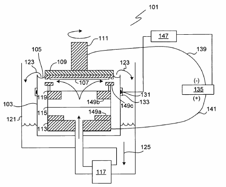
Manufacturing of semiconductor devices commonly requires deposition of electrically conductive material on semiconductor wafers. The conductive material. Such as cop per, is often deposited by electroplating onto a seed layer of copper deposited onto the wafer surface by a PVD or CVD method. Electroplating is a method of choice for depositing metal into the Vias and trenches of the processed wafer during damascene and dual damascene processing.
Damascene processing is used for forming interconnec tions on integrated circuits (ICs). Damascene processing involves formation of inlaid metal lines in trenches and vias formed in a dielectric layer (inter-metal dielectric). In a typi cal damascene process, a pattern of trenches and vias is etched in the dielectric layer of a semiconductor wafer sub strate. A thin layer of diffusion-barrier film such as tantalum, tantalum nitride, or a TaN/Tabi-layer is then deposited onto the wafer surface by a PVD method, followed by deposition of seed layer of copper on top of the diffusion-barrier layer. Typical materials for diffusion barrier layers include titanium (Ti), tantalum (Ta), tantalum nitride (TaN), tantalum nitride silicon (TaNSi), tungsten (W), titanium nitride (TiN), tita nium nitride silicon (TiNSi) and the like.
The trenches and vias are filled with copper mostly com monly using an electroplating process. Because electroplat ing must occur on a conductive layer, a copper seed layer is first deposited on the diffusion barrier layer with CVD or PVD methods. Chemical vapor deposition (CVD) methods can deposit a conformal copper seed layer with good adhe sion, but CVD methods are expensive as compared to PVD processes. Physical vapor deposition (PVD) methods can deposit a copper seed layer with good adhesion, but produces a less conformal film that covers the sidewalls and bottoms of trenches poorly. A thicker PVD seed layer is therefore required to ensure that an electrically conductive layer is provided for subsequent electroplating. The thicker PVD seed layer increases aspect ratios in features and may pinch off the gap opening, making the features harder or impossible to fill with an electroplating process.
As feature sizes decrease, the limitation of a PVD seed layer restricts how small metal lines can be. It is desirable to deposit a verythin copper seed film with good adhesion and conformality so that the aspect ratio of the remaining gap stays within a range that can be filled with an electroplating process. Accordingly, a method of Such deposition, and an apparatus allowing practice of Such a method, are needed.

Fig1
Manufacturing of semiconductor devices commonly requires deposition of electrically conductive material on semiconductor wafers. The conductive material. Such as cop per, is often deposited by electroplating onto a seed layer of copper deposited onto the wafer surface by a PVD or CVD method. Electroplating is a method of choice for depositing metal into the Vias and trenches of the processed wafer during damascene and dual damascene processing.
Damascene processing is used for forming interconnec tions on integrated circuits (ICs). Damascene processing involves formation of inlaid metal lines in trenches and vias formed in a dielectric layer (inter-metal dielectric). In a typi cal damascene process, a pattern of trenches and vias is etched in the dielectric layer of a semiconductor wafer sub strate. A thin layer of diffusion-barrier film such as tantalum, tantalum nitride, or a TaN/Tabi-layer is then deposited onto the wafer surface by a PVD method, followed by deposition of seed layer of copper on top of the diffusion-barrier layer. Typical materials for diffusion barrier layers include titanium (Ti), tantalum (Ta), tantalum nitride (TaN), tantalum nitride silicon (TaNSi), tungsten (W), titanium nitride (TiN), tita nium nitride silicon (TiNSi) and the like.
上一篇: 晶圆级芯片级封装的背面保护
下一篇: 单晶片炉的设计及在快速热处理中的应用