Abstract—A monolithic high-resolution (individual pixel size 300 × 300 µm2 ) active matrix (AM) programmed 8 × 8 microLED array was fabricated using flflip-chip technology. The display was composed of an AM panel and a LED microarray. The AM panel included driving circuits composed of p-type MOS transistors for each pixel. The n-electrodes of the LED pixels in the microarray were connected together, and the p-electrodes were connected to individual outputs of the driving circuits on the AM panel. Using flflip-chip technology, the LED microarray was then flflipped onto the AM panel to create a microdisplay.
The AM panel was fabricated with standard CMOS process on a (1 0 0) single crystal silicon wafer. After cleaning, well regions and body connection was defifined by ion implantation. Then, a layer of silicon nitride was deposited and patterned. Field oxidation was performed to defifine the active area of the transistors using silicon nitride as a hard mask. Then, a thin layer of thermal oxide was grown as gate oxide. After poly-Si deposition and gate patterning, source/drain region was formed by ion implantation with standard self-alignment technology. Then, low temperature oxide (LTO) was deposited, and the wafer was annealed to densify the LTO and to activate the implanted dopants simultaneously. After opening of contact holes on the LTO layer, Al–Si alloy was deposited, and patterned for source/drain electrodes and interconnections.
After the CMOS process, a layer of PECVD SiO2 was deposited on the AM panel for passivation and holes were opened. A TiW/Cu (30/500 nm) seed layer was deposited by sputtering and photoresist AZ4903 was coated and patterned by photolithography. A thick Cu layer (8 µm) and solder layer (22 µm) was deposited by electrical plating. After reflflow in the annealing furnace, excellent solder bumps were formed in ball shape, as shown Fig. 2. The LED microarray wafer was thinned and diced. After flflipping the diced LED microarray onto the AM panel, the fifinished device is shown in Fig. 3. The completed device was packaged in a dual in-line package (DIP) 40 socket and electrically connected by wire bonding.
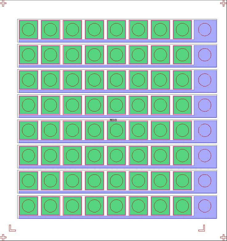
Fig. 4 shows the layout of the LED microarray. In our design, all individual LEDs (emission wavelength = 440 nm) on the same column are connected by the n-contacts at the end of each row as cathodes. The current passes through the n-GaN layer and the n-metal bus line to reach the n-contact. Individual LEDs on the same row are connected to the output of the AM panel through the solder bumps as anodes. The LED microarray has identical electrical properties as a commercial 8 × 8 LED dot array. As shown by commercial discrete power LED manufacturing, flflip-chip technology can improve heat dissipation, reliability, and manufacturability. Silicon has a larger thermal conductivity (150 W/m·K) than sapphire substrate (46 W/m·K), and well-developed flflip-chip technology has been used in silicon for decades. In the epi-down (bottom emitting) confifiguration, the p-contact itself can be made reflflective, thus eliminating any absorption of the current spreading layer and metal pads. In this way, the light output power and effificiency will be improved. The turn-ON voltages of LEDs, under the same 20 mA current injection, were strongly dependent on the distance between each LED and the n-contact. Series resistance of the bus bars to the n-GaN contact strip resulted in increased turn-ON voltage with longer distance of dies from the contacts at the end of each column [7]. For high-performance microdisplays, the variation of turn-ON voltage might cause a different junction temperature and/or a compensation of piezoelectric fifield between the individual LED pixels, and hence, a variation in lifetime and emitting wavelength. The later one would result in a poor angular homogeneity of color purity. In this study, the turnON voltage uniformity was greatly improved in a design with 40-µm-wide one-side n-metal bus lines on each row. The turnON voltages varied only from 3.30 to 3.70 V over the whole row under the same current injection, as shown in Fig. 5. Improved designs of the bus bars can be implemented in future versions to eliminate the variation completely.

Fig1
The confifiguration of the driving circuit on the AM panel is shown in Fig. 6. Transistor T1 serves as a switching transistor and T2 serves as a driving transistor. When T1 is switched on by a scan signal, a data signal would switch T2 on and be stored in the capacitor C1. Then, T2 would provide current to light up the LED pixel whose p-electrode was connected to the drain of T2. Driving transistor T2 was designed with a large W/L ratio to warrant enough output current for the LED pixel. Fig. 7 shows a typical I–V characteristic of an individual pixel in the AM LED array. Since the LED and the driving transistor are connected in series, the operating points are determined by the power supply voltage as well as the I–V characteristics of the LED and the driving transistor. From the I–V curve, we could fifind that the AM panel has suffificient driving capability for the LED microarray.
In summary, we have demonstrated a monolithic highresolution AM-programmed LED microdisplay by using flflipchip technology. The display has the advantages of high brightness, good luminance uniformity, and individual controllability. This paper shows that integration of GaN-based LEDs with the mature Si manufacturing technology is viable, and different lighting systems on a chip can be developed using similar technology. UV LED arrays are being fabricated for a full 12 × 12 Red, Green, Blue (RGB) AM panel for high-resolution, fullcolor LED microdisplays.
上一篇: 使用 UV LED 的无掩模光刻