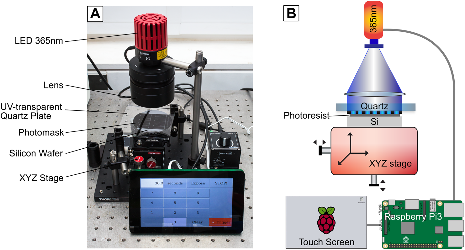
Current lithography approaches underpinning the fabrication of microflfluidic devices rely on UV exposure of photoresists to defifine microstructures in these materials. Conventionally, this objective is achieved with gas discharge mercury lamps, which are capable of producing high intensity UV radiation. However, these sources are costly, have a comparatively short lifetime, necessitate regular calibration, and require signifificant time to warm up prior to exposure taking place. To address these limitations we exploit advances in solid state sources in the UV range and describe a fast and robust wafer-scale laboratory exposure system relying entirely on UV-Light emitting diode (UV-LED) illumination. As an illustration of the potential of this system for fast and low-cost microflfluidic device production, we demonstrate the microfabrication of a 3D spray-drying microflfluidic device and a 3D double junction microdroplet maker device. Published by AIP Publishing.
Photolithography techniques that rely on transferring small scale structures from photomasks onto flflat substrates using light represent one of the main fabrication routes in microelectronics and micro-devices,1,2 including microflfluidics.3–5 Generally, radiation in the UV range is used to activate photoresists and the illumination is achieved commonly with gas-discharge lamps using mercury vapour. Such sources produce a wide spectrum of light and are coupled with fifilters to select the desired wavelength. Appropriate optics can then be used to collimate the light over the entire exposure area. However, such lamps require signifificant time to warm up, have a limited life time of typically 2000 hours for laboratory sources, and require regular calibration.
In an attempt to optimise the laboratory scale fabrication of microflfluidic devices, we have explored solutions to simplify the photolithography step by exploiting progress in solid-state light emitting diode (LED) sources operating in the UV range. There are several requirements for an effective and accurate UV exposure source for lithography applications. First, the light used for photolithography should be uniform over a wafer scale to maintain compatibility with standard wafer substrates and to ensure that each area is exposed to the same dose of energy. Second, the emission spectrum should have a small bandwidth since the absorption in the photoresist is wavelength dependent. Finally, the illumination should be well collimated to ensure sharply defifined features in the fabricated microstructures. All of these features can be achieved using light emitting diodes (LEDs) and UV transparent optical lenses. LEDs possess clear advantages over mercury lamps as they consume less electricity, they can be turned on and off within seconds, their life time is 20 000 hours, and they are cheap and extremely simple to use. However, until recently, the main limitation was their low power in the UV spectrum, which hindered their routine use for photolithography applications. This technical limitation has been overcome by assembling several LEDs into arrays. As such, new generation LED light sources have a high power source with integrated heat sink to keep the power at stable values, allowing their use for photolithography. We combine the exposure system with a micrometer positioning stage to allow multilayer lithography to be performed.
In view of the considerations above, we present here a highly versatile lab-scale UV-LED based photolithography set-up, with a mask aligner comprised of micrometric XYZ and rotation stages. The set-up addresses the main issues of conventional mercury lamp based mask aligners while retaining the resolution required for conventional microflfluidic applications. In this paper, we describe the entire set-up in Section II and its characterisation in Section III. We show some examples of the features obtained, and in particular, we show polydimethylsiloxane (PDMS) based microflfluidic devices fabricated with the set-up in Section IV.

Fig1
In this section, we discuss the characterisation of the set-up and show that the features obtained compare well with those obtained using a conventional mercury lamp, but with the advantages of low-cost, convenient and reliable operation characteristic of LED sources. To validate the performance of the UV-LED lithography platform, we have micro-fabricated structures into the negative SU8 3000 series(Microchem) i-line photoresist. The photoresist is spun onto a silicon wafer and soft baked according to the manufacturer’s protocols. The photomask with the desired patterns is then placed on the wafer and the whole assembly is positioned under our home built LED-lithography platform. Upon exposure, the UV light crosslinks the exposed SU8 photoresist and the unexposed SU8 is dissolved using appropriate solvents during the development step. After the post exposure bake, the SU8 patterns are visible on the wafer.