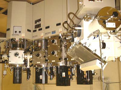
We have recently employed silicon micromachining technology to fabricate an organic semiconductors based light emitted diode on silicon substrate. Organic semiconductors are very promising for the electronic devices of the third millennium but currently suffer from technological process for the fabrication of devices. To overcome this difficulty we proposed to deposit both organic semiconductors and metals for electrical contacts through micromachined silicon shadow masks. Moreover, a micromachined silicon structure has been designed for the integration of the organic material based active device with electrical circuit or Micro Electrical Mechanical System.
Optical MEMS so called MOEMS are usually made by the integration of both optical, electrical and mechanical components in one microsystem and therefore are well known to be the key devices of high-performance systems in many applications as telecommunication, automotive Moreover, most of the MOEMS are developed on silicon as optical switch, micro optical bench.As for MEMS, the main reason is that silicon has consistently been the material of choice for the microelectronics industry, due to a mature processing technology which offers the possibility to integrate MEMS devices with Integrated Circuits in a low cost batch fabrication process. However, silicon has been suffering since the beginning of Optoelectronic from its poor efficiency to emit light because of its indirect band gap. It is the reason why most of the MOEMS are based, as for optoelectronic devices, on III-V material when the emission of light is required. The interest to combine both III-V and silicon technology remains very strong, and many works are developed in this direction.
Another alternative to integrate emitting devices on silicon is proposed in this work with the integration of organic semiconductor based emitting devices on silicon substrate. During the last decade, organic semiconductors have attracted increasing research interest from both academia and industry. Investigation of material properties, device structures and characteristics show that electronic and photonic devices can be successfully prepared from organic compounds. The most difficult operation is the fabrication of devices with good reliability. Among the different techniques developed for the deposition of polymeric films, Organic Molecular Beam Deposition (OMBD) technology allows the subsequent growth of thin solid films and was used for example to deposit organic semiconductor on III-V material for microwave application. For optical application with the fabrication of Organic Light Emitting Diode (OLED), most of the reported devices propose the deposition of organic semiconductor on glass, which is transparent at the working wavelength, usually in the visible range. A silicon-based organic light emitting diode has been reported, for operation at a wavelength of 1.5µm for which silicon is a transparent material. Lasing action in organic vertical-cavity surface-emitting laser was demonstrated around 500nm with optically pumped structures on quartz and one of the first organic semiconductorbased microcavities on silicon has been realised by a French Team from Lyon, LEOM where Massenelli and his co-worker deposited on silicon substrate all the active layers for a device which emits light at 515nm under optical pumping. As organic semiconductors are very attractive for their broad emission spectrum according to their chemical structures, the possibility to deposit any kind of OLED on silicon seems to be very attractive for both the integration of the electronic and the use of MEMS capability.

Fig1
The proposed silicon microstructure with the integration scheme of the OLED is given figure 3. As Silicon absorbs light until 1.1µm, the microstructure is based on a transparent membrane which has to be design thank to mechanical and process considerations. For the electrical aspect, the main interest of silicon micromachining with the well known anisotropic etching of silicon allows to realise the proposed shape in order to avoid any discontinuity in the electrical circuits for both ITO and Al pads.
This work reported a new method for the fabrication of Organic Light Emitting Diode on Silicon microstructure with the use of silicon micromachined shadow masks. The proposed concept should be useful for the integration of any kind of OLED deposited with Organic Molecular Beam Deposition technique, with silicon based MEMS and /or Integrated circuit.
The improvement of the proposed technique is going on, with the design of new silicon shadow masks, particularly to control the sputtering deposition through micromachined shadow mask, which is to our knowledge, proposed for the first time in this work. The second aspect is the design and fabrication of silicon microstructures to perform transparent membranes as large as possible, in order to control the injection of current in a homogenous organic semiconductor layer.
下一篇: MicroLED 的发射特性