Microscopic light-emitting diode arrays (microLEDs) are predicted to revolutionize the display technology market with boundless applications in portable electronics and wearable displays such as augmented reality headsets. MicroLEDs offer higher resolution and lower power consumption than traditional display technologies due to avoiding power losses associated with color conversion using phosphors. Recent development trends have seen microLED arrays evolve into close-packed three-dimensional structures that introduce photonic crystal (PhC) effects enabling researchers greater control of light emission properties. Novel optical devices employing photonic crystals and metamaterials have an abundance of potential applications which may be utilized to enhance microLED display technologies. PhCs and metamaterials take advantage of coherent scattering and near-field interactions, modifying microLED emission intensity and controlling the emission pattern(s).
PhCs can be designed with specific photonic band structures that selectively control the transmission or propagation of light at prescribed frequencies and directions defined by the PhC lattice form and periodicity. Therefore, optimizing devices with photonic enhancement necessitates experimental techniques that characterize their unique optical properties and correlate them with the physical structure. In this study, we introduce a technique to characterize the photonic band structure of a microLED fabricated as a PhC using an analysis method termed wavelength- and angle-resolved cathodoluminescence (WARCL) [1, 2] stimulated in a scanning electron microscope (SEM). The WARCL technique simultaneously reveals wavelength and angular anisotropy present in the emission of a specimen and enables researchers to relate those emission properties to the physical structure directly.
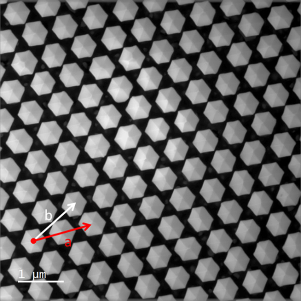
In this study, an array of core-shell GaN-InGaN multiple-quantum-well (MQW) micro-pillars were analyzed, which were grown using a hybrid bottom-down/top-up approach [3]. The pillars were nominally 470 nm wide and arranged in a 2-dimensional triangular lattice with a 650 nm pitch, see Figure 1. The micro-pillars in the triangular array lattice demonstrated a variance in micro-pillar shape with a facet length of 250 ± 50 nm. The triangular lattice was stretched along one direction with periodicity and the triangular lattice directions of 510 ± 5 nm and 570 ± 5 nm (along the a-direction).

Fig2
A spectrum image of a single pillar, displayed in Figure 2, revealed intense CL emission across the visible spectrum (350 – 700 nm) with significant spatial variation. Analysis of the emission spectrum revealed luminescence associated with the GaN (band edge at 365 nm and sharp yellow band at 540 nm) and a ‘bundle’ of peaks at 450 – 475 nm. The complex spectral behavior observed at wavelengths >400 nm was not observed from isolated pillars (e.g., not part of the array) and, therefore, could be attributed to interference and photonic effects imposed by the array lattice.
The emission anisotropy by wavelength and angle was observed by WARCL, where the excited pillar ensemble demonstrated a strong variation in the emission pattern across the visible range of wavelengths, see Figure 3. Significant variation in emission pattern was observed across multiple micro-pillars due to the micro-pillar shape through boundary refraction and the effects of optical interference from the array. The PhC related emission anisotropy was more intense at shorter wavelengths (higher energy) but did not influence the GaN band edge emission at 365 nm (3.40 eV). This is not unexpected since the micro-pillars are mostly GaN and the micro-pillar lattice period is larger than the band edge emission wavelength. The influence of the triangular lattice stretching can be observed in the WARCL emission patterns more prominently at 2.48 and 2.34 eV, displayed in Figure 3.
下一篇: 用于LED表征的光学显微镜和光刻