We demonstrate capabilities of near-field scanning optical microscopy (NSOM) in collection and illumination mode. NSOM in collection mode was used for high resolution characterization of optical field of patterned light emitting diodes. In the scanned near field, we resolved enhanced emission from patterned regions with high resolution images of emitting surface. Also NSOM in illumination mode was used for patterning of predefined structures on semiconductor surfaces. For the diode patterning the electron beam direct writing lithography was used. Using NSOM lithography we prepared predefined planar structures in GaP surface. In the small open areas of predefined surface structure GaP nanowires were grown.
Near-field scanning optical microscope (NSOM) is an advanced diagnostic for the high resolution characterization of the optical fields. Typical NSOM arrangement employs fiber probe in collection mode, thus detects the light intensity in the near field of the emitting objects. The collection mode of NSOM is standardly used for analysis of light emitting objects with dimensions under the Rayleigh diffraction limit of standard optical microscopies. Later, NSOM experiment was successfully used in illumination mode as a promising lithography technique for two-dimensional (2D) planar structure fabrication. The patterning of structures is done through a direct writing process performed by the optical near-field produced at the tip of a fiber probe. Here, we use NSOM as characterization and lithography technique for fabrication of surface photonic structures in GaP surface for organized nanowires (NWs) growth and also for analysis of optical field of patterned surface of light emitting diodes (LED).
Extraction efficiency improvement as well as radiation pattern modification of LED was well described while using planar photonic structures in the surface of the device. We analyze a quantum well LED with 2D surface structure of square symmetry in periodic arrangement patterned by electron beam direct writing (EBDW) lithography. Light produced in active region of a conventional LED is outcoupled from the surface with considerable losses given by total internal reflection on semiconductor/air interface. Typically for GaAs based LEDs these losses achieve more than 30% of light. Many of groups have demonstrated way to improve light extraction efficiency from the LED surface if the surface is patterned. Here, the NSOM can bring useful information about local enhancement of light emission from the patterned regions in comparison with the surrounding surface.

Fig1
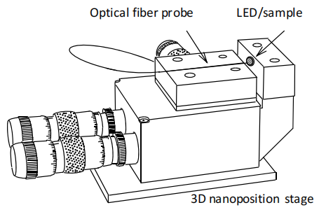
Experimental arrangement for NSOM analysis and lithography is shown in Fig. 1. Experimental stage for NSOM analysis requires high resolution 3D nanoposition system (in closed loop mode < 5 nm) controlled by computer. A Lock-In technique with Si femtowatt detector was used for signal detection and pulse-supply system for the LED driving. For the near-field scanning, the fiber probe was placed in the vicinity of the LED surface (< 200 nm). Optical field of the LED was obtained by scanning the intensity from the emission part of the LED surface. Synchronization of motion and signal detection is controlled via LabView program.
NSOM lithography uses the same 3D axis nanoposition piezosystem. As a local exposure source the apertureless optical fiber is used. Modulated 473 nm diode-pumped solid state laser was used as a light source. The laser beam was focused by micro objective into conventional optical fiber, which was coupled to the fiber probe fixed on the 3D axis nanoposition piezosystem. Synchronization of motion and exposure is controlled via LabView program.
The fiber probe realized the in-plane movement over the sample in the non-contact mode in the near field of the fiber probe. As a fiber probe, a home-made fiber tip prepared by etching of the conventional optical fiber in hydrogen fluorid acid was used. In the next step, the fiber tip was coated by Al evaporation. The technology produces apertureless optical fiber probes with resolution better than 300 nm, what limits the overall resolution of the NSOM system.
上一篇: MicroLED 的发射特性