Photonic integrated circuits offer the potential of realizing low-cost, compact optical functions. Silicon-on-insulator (SOI) is a promising material platform for this photonic integration, as one can rely on the massive electronics processing infrastructure to process the optical components. However, the integration of a Si laser is hampered by its indirect bandgap. Here, we present the integration of a direct bandgap III-V epitaxial layer on top of the SOI waveguide layer by means of a die-to-wafer bonding process in order to realize near-infrared laser emission on and coupled to SOI.
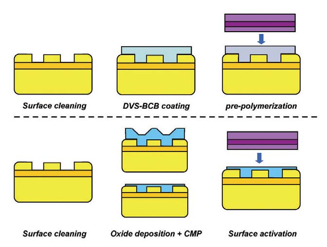
Two techniques for semiconductor wafer bonding have been investigated. In the first approach, adhesive semiconductor wafer bonding18 using the thermosetting polymer divinylsiloxanebenzocyclobutene (DVS-BCB) as a bonding agent has been developed, while in the second approach, molecular wafer bonding has been investigated20. Both approaches are schematically outlined in Fig. 3.
In adhesive wafer bonding, an oligomer solution of DVS-BCB is spin coated onto the processed SOI waveguide circuit. This process planarizes the waveguide topography. After spin coating, a baking step at 150°C removes residual solvent in the spin-coated film, while a short baking step at 250°C transforms the liquid DVS-BCB into a sol/gel rubber by partial polymerization. The preparation of the InP/InGaAsP epitaxial layer surface is optimized to achieve a high bonding strength. A HF surface treatment improves the bonding strength by chemical modification of the III-V surface. After attachment of the III-V dies, the wafer stack is cured at 250°C for 1 hour to polymerize the DVS-BCB completely. A uniform pressure is applied to the wafer stack during curing to achieve a close contact between both surfaces. DVS-BCB was chosen as the bonding agent because of its optical transparency, excellent planarization properties, low curing temperature, the fact that no outgassing occurs during cure, and its high glass transition temperature (>350°C), which determines the available post-bonding thermal budget for the fabrication of the laser diodes.
In the molecular wafer bonding approach, the processed SOI wafer surface is coated with an SiO2 cladding layer and planarization is achieved by chemical mechanical polishing (CMP). Subsequently, the III-V epitaxial layer structure is coated with SiO2 and, if needed, a touch-polish CMP step can be used to reduce the surface microroughness, necessary to achieve molecular bonding. This is because of the short range of the van der Waals attraction forces on which the molecular bonding relies. For the approach to be successful, the surfaces of both wafers must be in contact on the atomic scale. Typically, a root mean squared (RMS) microroughness of 0.5 nm is required to achieve molecular adhesion. After surface planarization and reduction of the microroughness by CMP, both wafer surfaces are chemically activated. Hydrophilic SiO2 surfaces can be achieved by both wet chemical treatment and plasma activation. Van der Waals interactions between both surfaces is achieved when the two activated wafer surfaces are attached to each other because of the presence of a H2O interface layer, which is readily adsorbed at the wafer surface. During annealing of the bonded stack, H2O molecules are removed from the bonding interface, leaving a covalent bond between the SiO2 surfaces. In other work, the processed SOI waveguide is not planarized and the III-V die is directly bonded onto the SOI waveguide topography, leading to air gaps in the bonded stack.

Fig3
After bonding of the III-V dies to the SOI waveguide wafer, the InP growth substrate is removed using a combination of mechanical grinding and wet chemical etching using 3HCl:H2O until an InGaAs etch stop layer is reached. After substrate removal, the bonded epitaxial layer stack is ready for device processing. An example of an InP/InGaAsP epitaxial film transferred to an SOI waveguide circuit using DVS-BCB is shown in Fig. 4.
While this approach requires a dedicated structure to couple light from the III-V layer to the SOI waveguide circuit, because of the presence of the DVS-BCB bonding layer, the use of hybrid waveguide structures, in which the laser waveguide mode is partially located in the Si waveguide core while it experiences gain from the III-V layer, has been demonstrated as well in other work. This approach, however, relies on a relatively thick Si waveguide core layer (690 nm). Scaling this approach to Si waveguide core layers λ/2n thick as used in this work, which are required for high density integration, is not straightforward.
上一篇: 在氮化硅蚀刻期间提高蚀刻选择性的方法
下一篇: ECR等离子蚀刻和湿化学蚀刻的比较