Fabrication of semiconductor devices is a multi-step pro cess of forming features on a semiconductor Substrate or other Substrate. Steps can include material growth, pattern ing, doping, deposition, etching, metallization, planarization, and so forth. Features formed on a substrate can include various transistors. Transistors can be planar or non-planar, and can also have single gates or multiple gates. Non-planar transistors (sometimes referred to as 3D transistors) include the FinFET (fin field effect transistor), among others. Such non-planar transistors typically include a vertically-oriented or raised fin that functions as a channel between the Source and drain. The gate is also vertically-oriented or raised and is positioned over the fin (on top of the fin and around fin sidewalls). Such non-planar transistors can have multiple fins and/or multiple gates. Planar transistors also have associated heights, though relative heights of non-planar features are usually greater than those of planar transistors.
Fabrication of semiconductor devices often includes depo sition of spacer and/or dummy materials to assistin construct ing a given feature design, including features on non-planar transistors. Sidewall spacers are often specified on non-planar transistors for improved gate functionality. As the dimensions of the transistor gate continue to shrink, the fringe capaci tance between the gate and contact, as well as between the gate and facet of the source/drain (S/D), has increased. To counter this increase in fringe capacitance, low-k dielectric materials have been implemented as the spacer material. The Success of a spacer is affected by a spacer etch process, which can affect both the dielectric constant of the spacer, as well as Spacer coverage.
During fabrication of a transistor gate, a spacer material is conformally applied to the transistorgate and other structures (such as by atomic layer deposition), and then partially removed to form a sidewall spacer on a sidewall of the tran sistor gate. This partial removal step specifies removing spacer material from the other structures, while leaving spacer material on the gate or on gate sidewalls. Such partial removal is typically executed using one or more etching pro cesses, but can be challenging because of the differing heights of features being etched simultaneously as well as thick nesses of spacer material.
Techniques herein include methods to increase etch selec tivity among materials. Techniques herein include a cyclical process of etching and oxidation of a silicon nitride (Sin) spacer and silicon (such as polycrystalline silicon). This tech nique can increase selectivity to the silicon so that silicon is less likely to be etched or damaged while silicon nitride is being etched from sidewalls. Techniques and chemistries as disclosed herein can be more selective to silicon oxide and silicon as compared to silicon nitride. An oxidizing step cre ates an oxide protection film on silicon Surfaces that is com paratively thicker to any oxide film formed on nitride sur faces. As such, techniques herein enable better removal of silicon nitride and silicon nitride spacer materials.

Fig1
Techniques herein include methods to increase etching selectivity among materials. Techniques herein include a cyclical process of etching and oxidation of a silicon nitride (SiN) spacer and silicon (Such as polycrystalline silicon). This technique can increase selectivity to the silicon so that silicon is less likely to be etched or damaged while silicon nitride is etched from sidewalls and other surfaces. Tech niques and chemistries as disclosed herein can be more selec tive to silicon oxide and silicon as compared to silicon nitride. An oxidizing step creates an oxide protection film on silicon Surfaces that is comparatively thicker to any oxide film formed on nitride Surfaces. As such, techniques here enable better removal of silicon nitride and silicon nitride spacer materials.
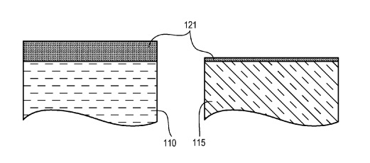
Improved removal of silicon nitride is enabled in part based on discoveries herein that silicon material (crystalline silicon) oxidizes at a faster and/or thicker rate as compared to oxida tion of silicon nitride. Thus, methods herein include a process ofetchingaportion of spacer material followed by a relatively short oxidation step, and then returning to etching a Subse quent portion of spacer material. This etching-oxidation cycle can be repeated until meeting a design specification Such as removing conformal spacer material from around a given structure. In other words, periods of etch activity followed by periods of protection are cycled. The result of such methods and discoveries herein can include better etch selectivity, as well as uncovering fin structures with more fin material remaining as compared to conventional processes.
下一篇: 通过晶圆键合的硅光子学