A method and system for cleaning and/or stripping photo resist from photomasks used in integrated circuit manufac turing comprising a process and means of introducing a mixture of sulfuric acid and ozone (or a mixture of sulfuric acid and hydrogen peroxide) to the Surface of a photomask while applying megaSonic energy. The invention also com prises method and system comprising a process and means of introducing oZonated deionized water and/or a low tem perature dilute aqueous solution (dAPM) to the surface of photomasks while applying megaSonic energy. The process and apparatus also remove post plasma ashed residues and other contaminants from photomask Surfaces.
process that includes a photolithographic processing step. A photolithographic process step uses photomasks (or reticles) in combination with a light Source to optically project a circuit image onto the Surface of a silicon wafer or Substrate that has a light-sensitive layer, such as photoresist, applied to its Surface. A photomask is a transparent ceramic Substrate that is coated with a metallic layer forming a pattern for an electronic circuit. During the manufacture of ICs, a pellicle is typically used to seal the photomask from particulate contamination, thereby isolating and protecting the photomask surface from dust or other particles from the focal plane of the photomask pattern.
In order to produce functioning ICs at a high yield rate, the photomask and pellicle need to be free of contamination. Contamination of the photomask can occur both during the manufacture of the photomask itself, and during use of the photomask in the IC manufacturing process, specifically during processing and/or handling of the photomask. One type of contamination is organic/molecular contamination of the photomask Surface. Organic/molecular contamination, Such as chemical stains or residues, on the Surface of the photomask reduces and degrades the transmittance property and/or characteristic of the photomask, ultimately impacting the qual.
Cs during the photolithography process is particulate con tamination. Particulate contamination may include any Small particles, such as dust particles, that may be on the photo mask or caught between the photomask and the pellicle. Particulate contamination may cause the photolithographic pattern transmitted on the wafer to change, distort, alter, etc. from its intended design, ultimately impacting the quality of the semiconductor device manufactured.

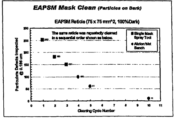
Fig1
Still another aspect of photomask manufacturing process which is known to affect the quality of the circuit patterns projected during photolithography is the stripping of pho toreist from the photomask surface. Similar to the manufac ture of the IC devices, during the manufacture of the photomask, photoresist is applied to Surface of the photo mask and light and/or ultraviolet radiation is applied to the photomask Surface in a desired circuit pattern. Once the exposure is completed, the photoresist is removed from the surface of the photomask, thereby revealing the circuit pattern. Proper removal of photoresist is required so as to ensure that the circuit pattern is not changed, distorted, altered, etc. from its intended design.
上一篇: 使用超临界二氧化碳进行精密表面清洁
下一篇: 在氮化硅蚀刻期间提高蚀刻选择性的方法