REBL (Reflective Electron Beam Lithography) is being developed for high throughput electron beam direct write maskless lithography. The system is specifically targeting 5 to 7 wafer levels per hour throughput on average at the 45 nm node, with extendibility to the 32 nm node and beyond. REBL incorporates a number of novel technologies to generate and expose lithographic patterns at estimated throughputs considerably higher than electron beam lithography has been able to achieve as yet. A patented reflective electron optic concept enables the unique approach utilized for the Digital Pattern Generator (DPG). The DPG is a CMOS ASIC chip with an array of small, independently controllable cells or pixels, which act as an array of electron mirrors. In this way, the system is capable of generating the pattern to be written using massively parallel exposure by ~1 million beams at extremely high data rates (~ 1Tbps). A rotary stage concept using a rotating platen carrying multiple wafers optimizes the writing strategy of the DPG to achieve the capability of high throughput for sparse pattern wafer levels. The exposure method utilized by the DPG was emulated on a Vistec VB-6 in order to validate the gray level exposure method used in REBL. Results of these exposure tests are discussed.
Electron Beam Lithography (EBL) is well known to produce excellent resolution, good line edge roughness (LER) and good line width roughness (LWR) at the cost of throughput. The cost paid by throughput is because the electron dose must be high enough to mitigate the statistical effects of the electron beam (shot noise) and of the resist and developing process, to achieve an acceptable LER/LWR. Unfortunately, with increased beam current comes increased beam blur as a result of the electron-electron coulomb interaction 1, 2 within the beam. Presently, it can take many hours to expose a wafer level using EBL systems. The REBL (Reflective Electron Beam Lithography) Nanowriter has the potential to break through the traditional performance/throughput tradeoff and achieve economically attractive throughputs while maintaining the advantage of maskless lithography.
EBL has for many years tried to become a major competitor in the lithographic market but has not succeeded in any meaningful way outside certain specialized markets. Mask making 3 is the most notable case. Another is high resolution lithography and personalization for specialized products. Quick-Turn-Around of small lot manufacturing has also proven to be quite successful. Two competing Electron Projection Lithography (EPL) programs for high throughput manufacturing, SCALPEL and PREVAIL developed starting in the early 90’s, did not utilize maskless technology and for various market reasons were never adopted by the semiconductor industry.

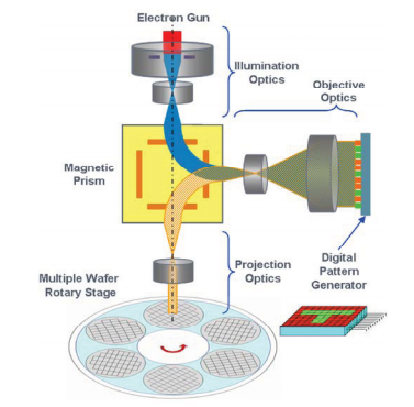
Fig1
Figure 1 depicts the system concept of the REBL Nanowriter. Six core technologies will be discussed in this paper: reflective electron optics, the Digital Pattern Generator, Time Domain Integration, gray tone exposure, the rotary stage, and optical wafer registration.
The DPG further provides for a rather sophisticated network of logic control that enables Time Domain Integration (TDI) & gray tone exposure without overburdening the data path and data transmission rate. TDI integrates the electron contribution of 248 beams in the TDI scan direction. This reduces the brightness requirements by over two orders of magnitude and distributes the exposure time over several microseconds, greatly reducing instantaneous resist heating effects. Gray tone exposure will be used to produce patterns with the required resolution, placement accuracy and pattern fidelity with a much finer incremental edge placement resolution than a larger size binary pixel would allow.
The rotary stage removes the throughput barriers normally associated with linear stages conventionally used in wafer lithography. This is especially important when a relatively small swath (few 100’s of microns in height) is used during the exposure process. In addition, it behaves quasi-statically, imparting virtually no disturbances to the system during the writing process. In fact, it is self-stabilizing. One could greatly reduce the demands on a linear stage by adopting a very large swath height, that is, expose a very large area with each pass of the stage. This was expressly ruled out during the concept and architectural phase of the REBL program because it was considered much more difficult to maintain beam calibration over such a large area during the exposure process. The exposure of a large swath height at greatly slower stage speeds, also produces heating effects in the wafer which can significantly alter the beam to beam calibration.
上一篇: ECR等离子蚀刻和湿化学蚀刻的比较
下一篇: 使用无线探头卡的非接触式晶片探头