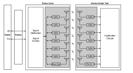
A method for wireless, non-contact testing of semiconductor wafers is presented. The technology applies to chips with active electronics, including standard integrated circuits (ICs), which require testing at the wafer level. The technology relies on short-range, near field communications to transfer data at gigabit per second rates between the probe card and the device under test (DUT) on a wafer. The probe consists of a CMOS device with micro antenna structures and transceiver circuits. Each antenna and transceiver circuit is capable of probing one input/output (I/O) site on the DUT. Each I/O site on the DUT is connected to a single antennae and transceiver circuit, which is designed into the DUT. The antennae and transceiver circuits can be incorporated into the DUT without any impact on performance or real estate. The main advantage of non-contact wafer probing is higher reliability (less retest, no pad scrub marks), added functionality (higher test frequencies at higher pin densities), and increased throughput (higher parallelism, reduced alignment tolerance, less maintenance, and less downtime). The wireless probes interface to standard automated test equipment (ATE) while all antenna structures and electronics needed on the DUT are fully CMOS compliant.
The testing of semiconductors is a significant and growing problem in the very large scale integration (VLSI) circuit manufacturing industry. With growing complexity and density of devices per wafer area, the cost of testing a microchip is growing faster than the cost of manufacturing one; and in some cases, the testing cost exceeds the manufacturing cost. Semiconductor testing has become a multi-billion dollar industry, leading to opportunities for the introduction of new testing technologies, like the wireless testing methodology. Issues such as smaller pad size, increased pad density, increased signal input/output (I/O) frequencies, longer test times, mechanical reliability of low-k dielectric materials, and probe card contact and alignment are restricting the progress towards smaller, faster, and more economical integrated circuits.
Wireless, non-contact testing alleviates all of these constraints, allowing for significant improvements in both the economics of integrated circuit manufacturing and the functional performance of the devices. In addition to the traditional testing performed at the end of the fabrication process (wafer probing or sort testing), wireless testing can also be implemented earlier in the manufacturing value chain, providing important feedback during the production process. This feedback relays information regarding any global or local physical faults, and even circuit-level faults, providing the process engineer the ability to respond earlier, leading to an improvement in yield. In addition, for mature processes, only a small statistical representation of devices on a wafer is tested prior to packaging (an expensive stage of manufacturing). Wireless testing, being a much faster process and capable of highly parallel testing, allows for increased test coverage on a larger population of devices, while maintaining throughput.

Fig1
The performance of the antenna structures and transceiver circuits have been modeled and simulated. For the antennae, the simulations were performed using a combination of four different simulation software packages. The first two packages, Totem (developed in an academic environment) and AxFDTD use the Finite Difference Time Domain (FDTD) method. The third and fourth packages were, Advanced Design System (ADS) and Sonnet, which use Method-of-Moments (MoM) analysis. Different simulations were run on each of the different packages to determine the optimum antenna geometry, antenna pitch, antenna size, matching circuits, and antenna termination. The results of the simulation were used to select the types of antenna that were most suitable for data and power transfer. Fig. 3 is the simulation model.
The simulation results demonstrate that the performance of the antenna is influenced by many factors. The antenna pair is optimized for operation with a 5 GHz carrier. The transmission coefficient (S21), for a pair of data transfer antennae (Type 3) is approximately -32 dB at 5 GHz and a separation distance of 60 µm. In Table 3, the cross-talk between adjacent elements is much greater than that the cross-talk between the elements in an echelon. The difference between required transmission efficiency (S21) and cross-talk (S31) is 18 dB when the horizontal separation distance is 60µm. As the distance is decreased to 30 µm, S31 increases 6 dB; however, S41 remains almost the same as for that of the greater channel distance. Due to this result, S31 is the main contributor of cross-talk. Some strategies for decreasing cross-talk will be discussed on Section 4. Electromagnetic simulation was used to determine the antenna type that would work the best for data and power transmission. Guided by the simulation results, the antenna pairs were optimized to operate at 5 GHz..