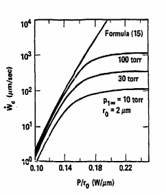
Mechanisms for laser-driven pyrolytic deposition of micron-scale metal structures on crystalline silicon have been studied. Models have been developed to predict temporal and spatial properties of laser-induced pyrolytic deposition processes. An argon ion laser-based apparatus has been used to deposit metal by pyrolytic decomposition of metal alkyl and carbonyl compounds, in order to evaluate the models. These results of these studies are discussed, along with their implications for the high-speed creation of micron-scale metal structures in ULSI systems.
In order that state-of-the-art computers can reproduce with less human interference and thus with lower error rates and latencies, it is necessary for them to be able to micropattem semiconductor substrata directly and at high speed. Contemporary supercomputer systems composed of 10s transistors, each constituted of as many as 10* 'tiles' of various materials stacked in particular arrangements, contain as many as io1 0 'tiles' in their ultra-large scale integrated (ULSI) patterns. In order that latencies involved in computer-directed generation of new computer-scale micropatterns be not much greater than a day, creation of a single 'tile' must be accomplished in an interval of the order of 13~5 seconds.
Monolithically implemented computers of the present era consist of sheets of metal traces of micron-scale width and thickness, separated almost (but not quite) everywhere from each other by nearly hole-free dielectric sheets, and occasionally touching the terminals of transistor devices which are embedded for convenience in a semiconductor substrate common to all such devices. The large majority of the structure (indexed by the fraction of total 'tiles' in the pattern) of computers implemented in the ever more popular metal-oxide semiconductor (MOS) family of technologies is expressed in metal (or in surrogate metal, highly doped polysilicon). It is thus quite crucial to greatly extend the hitherto highly limited ability to create suitable metal microstructures directly with laser processing techniques, as this approach is qualitatively superior to all other current prospects for high-speed, computer-controlled micropatteru generation directly on semiconductor substrates.
We report here an order of magnitude enhancement in the rate of metal micropatternin£ in the ULSI context, relative to the highest rates previously reported. Taken together with results from other workers on rapid semiconductor substrate doping and dielectric layer creation, this advance makes feasible in principle the generation of monolithic, ULSI supercomputers on day time scales.

Fig1
Desired metal patterns (frequently lines) were created by moving the reaction cell with an x-y table stepper drive (1 pm steps; 1500 pmjtec maximum speed), and by amplitude modulating the argon-ion laser beam by an optics chain which often included a halfwave plate followed by an electro-optics switch that was sandwiched between two GlanThompson prisms. During the course of each run, the laser patterns on the substrate and the deposited metal features were viewed through a microscope via a vidicon outputting to a color monitor. Laser beam profiles on the substrate were measured using a pinholephotodiode arrangement mounted on a calibrated x-y drive located after the microscope. The samples were analyzed using optical and scanning electron microscopy (the latter with X-ray fluorescence capability) and stylus profilometry.
Variations in height within a given metal line and between different lines drawn under similar conditions are attributed to the nature of nucleation on the surface. At lower power levels, the method of surface preparation (various methods of cleaning polished Si surfaces covered by its native oxide, including cleaning and stripping away the Si02 ) greatly affected the production of nucleation sites. Prenucleation due to boiling of metal from nearby nickel lines was observed to greatly lower the nucleation threshold for subsequent low laser power pyrolytic metal deposition runs. Nucleation effects are expected to be of much less importance in planned work involving substrate temperatures raised to far above threshold temperatures for sub-microsecond periods.
上一篇: 使用无线探头卡的非接触式晶片探头
下一篇: 晶圆级石墨烯的红外光谱