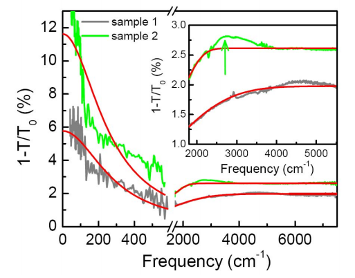
We report on spectroscopy results from the mid- to far-infrared on wafer scale graphene, grown either epitaxially on silicon carbide, or by chemical vapor deposition. The free carrier absorption (Drude peak) is simultaneously obtained with the universal optical conductivity (due to interband transitions), and the wavelength at which Pauli blocking occurs due to band filling. From these the graphene layer number, doping level, sheet resistivity, carrier mobility, and scattering rate can be inferred. The mid-IR absorption of epitaxial two-layer graphene shows a less pronounced peak at 0.37 ±0.02 eV compared to that in exfoliated bilayer graphene. In heavily chemically-doped single layer graphene, a record high transmission reduction due to free carriers approaching 40% at 250 μm (40 cm-1) is measured in this atomically thin material, supporting the great potential of graphene in far-infrared and terahertz optoelectronics.
As pristine graphene is gapless and a tunable, moderate band gap can be engineered using symmetry breaking schemes, it exhibits particularly strong potential in far-IR and terahertz optoelectronics.15 Characterization of wafer-scale graphene in the IR and terahertz range is a crucial step in the development of graphene optoelectronic devices. Previously, broadband optical absorption measurements of few and multilayer epitaxial graphene down to the terahertz range provided useful information of layer number as well as doping levels.Large area graphene samples produced by chemical vaporphase deposition (CVD) were also studied.The free carrier response of back-gated CVD graphene devices in the far-IR was carefully examined by Horng et al. 18 for carrier densities below 71012 cm -2. A reduction of Drude weight was observed.
Finally, a few comments should be made to the carrier scattering rate . The two epitaxial samples have similar scattering rate of ~270 cm-1, which corresponds to a scattering time of 20 femto-seconds. The CVD graphene has smaller scattering rate of ~100 cm-1 (scattering time of ~50 femto-seconds) and it doesn’t increase with the presence of chemical absorbates from the chemical doping. The difference for the scattering rate between epitaxial and CVD graphene can be due to the different sample quality, the surface morphology, and the doping concentration. The scattering times measured here are consistent with transport measurements.

Fig2
The red curve in far-IR is the fitting based on Drude model using parameters presented in the main text. Less noise in the far-IR spectrum than that in Fig. 2 is due to the higher light source power used. Inset: the enlarged view of the spectrum in mid-IR region with a sketch for the interband transitions. Red curve is the fitting based on Pauli blocking in mid-IR. The blue line is the universal interband absorption for single layer graphene on quartz. 2EF is indicated by the grey arrow. The Dirac cone of graphene is also shown in the inset. Photons with energy smaller than 2EF can not be absorbed by graphene due to Pauli blocking.
To conclude, we demonstrate that infrared spectroscopy is an excellent technique to characterize wafer-scale graphene in a non-invasive manner. We show that through the analysis of the absorption spectra in mid- and far-IR ranges simultaneously, layer number, doping, sheet resistivity, carrier mobility, and scattering rate can be inferred. For chemically doped CVD graphene, the reduction of transmission in far-IR in this atomically thin film approaches 40%, demonstrating the great potential of this novel two dimensional material in far-IR and terahertz applications, such as terahertz detectors and imagers.
上一篇: 晶圆级激光光刻
下一篇: 用于集成电路制造的压印光刻