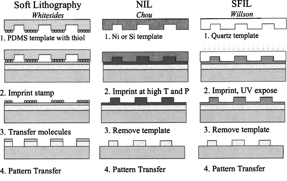
The escalating cost for next generation lithography ~ NGL! tools is driven in part by the need for complex sources and optics. The cost for a single NGL tool could exceed $50M in the next few years, a prohibitive number for many companies. As a result, several researchers are looking at low cost alternative methods for printing sub-100 nm features. In the mid-1990’s, several research groups started investigating different methods for imprinting small features. Many of these methods, although very effective at printing small features across an entire wafer, are limited in their ability to do precise overlay. In 1999, Colburn et al. @ Proc. SPIE 379 ~ 1999!# discovered that imprinting could be done at low pressures and at room temperatures by using low viscosity UV curable monomers. The technology is typically referred to as step and flflash imprint lithography. The use of a quartz template enabled the photocuring process to occur and also opened up the potential for optical alignment of the wafer and template. This article traces the development of nanoimprint lithography and addresses the issues that must be solved if this type of technology is to be applied to high-density silicon integrated circuitry.
In the fifields of micro- and nanolithography, major advancements in resolution have historically been achieved through use of shorter wavelengths of light. Using phase shift mask technology, it has already been demonstrated that 193 nm photolithography can produce sub-100 nm features. Along this path, such improvements come with an everincreasing cost for photolithographic tools. As conventional projection lithography reaches its limits, Next generation lithography (NGL) tools may provide a means to further pattern shrinks, but are expected to have price tag that is prohibitive for many companies.
The development of both light sources and optics to support the sources are primarily responsible for the rise in the cost of an NGL tool. 157 nm lithography, for example, requires the use of CaF2 as a lens material. In the case of extreme ultraviolet lithography, no source with suffificient out put has yet been identifified that will meet the industry’s throughput requirements.

Fig1
The step and repeat system was built at the University of Texas in Austin by modifying a 248 nm Ultratech stepper that was donated by IBM {see Fig. 2a} . Key system attributes include a microresolution z stage that controls the imprint force, an automated x – y stage for step and repeat positioning, a precalibration stage that enables parallel alignment between the template and substrate, a fifine-orientation flflexure stage that provides a highly accurate automatic parallel alignment of the template and wafer, an exposure source that is used to cure the etch barrier, and an automated flfluid delivery system that accurately dispenses known amounts of the liquid etch barrier.
Although the Imprio 100 from MII is a substantial improvement relative to the fifirst University tool, it has neither the throughput nor the overlay specififications necessary for silicon IC fabrication. Instead, the system was primarily designed and manufactured to address the compound semiconductor and photonics markets. These markets require high resolution features but are typically less sensitive to defects. They also operate at low volumes of wafers and are hence more sensitive to costs; particularly tool costs. The tool has a throughput capacity of approximately six 200 mm wafers per hour. As a result, it will be possible to collect enough statistical information of performance characteristics of S-FIL to allow the design of a fully engineered high volumemanufacturing tool in the future.
上一篇: 晶圆级石墨烯的红外光谱
下一篇: 用于高性能硅光子电路的浸没式光刻