Large-scale photonics integration has been proposed for many years to support the ever increasing requirements for long and short distance communications as well as package-to-package interconnects. Amongst the various technology options, silicon photonics has imposed itself as a promising candidate, relying on CMOS fabrication processes.. While silicon photonics can share the technology platform developed for advanced CMOS devices it has specific dimension control requirements. Though the device dimensions are in the order of the wavelength of light used, the tolerance allowed can be less than 1% for certain devices. Achieving this is a challenging task which requires advanced patterning techniques along with process control. Another challenge is identifying an overlapping process window for diverse pattern densities and orientations on a single layer.
Next-generation silicon photonics transceivers will require the integration of ultra-low-power active devices with ultralow-loss passive devices enabling wavelength-division multiplexing (WDM). A major challenge in the manufacturing of such devices is the extreme sensitivity of the device and waveguide properties (phase and amplitude transfer control) on the cross-sectional dimensions and sidewall quality of the employed photonic wire and rib structures, which results in poor device uniformity across a die or a wafer. Recently, there have been works reported on high-resolution pattering for silicon photonic circuits by using advanced CMOS technology . Since it is early days, the performance reported so far are on-par with 200mm based toolset. In this paper, we demonstrate that by using advanced CMOS process technology with 300mm pattering toolset performance and device can be improved by an order of magnitude.
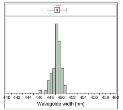
Patterning of silicon photonic circuits bring new challenges compared to CMOS, in particularly for lithography. The two main challenges for lithography are, firstly, diversity in device geometry, where a ring resonator is defined by a combination of an isolated line, which is ~450 nm and a semi-isolated trench of ~140 nm. Another example of such diversity is photonic crystal devices, where one would need an isolated line and dense holes. Though the CDs, at least in the present example do not call for advanced patterning platform the specification on the dimensional accuracy and tolerance is demanding. Silicon photonic devices are very sensitive to small cross-section dimensional variation, roughly 1nm variation in CD would shift the spectral response of the device by 1nm. Hence a platform that can deliver such a high degree of uniformity is needed. Though active tuning can be employed, it is desired that the CD variation is kept to a minimum to reduce power spent on tuning the non-optimal devices. In addition, line edge roughness on the waveguides both high and low-frequency components of roughness directly affect the optical propagation loss in the waveguides by scattering along the edges of the patterned silicon. The loss in the optical power has a direction implication on the power penalty of the systems, hence the loss has to be controlled, particularly where energy efficiency is crucial.
The devices were fabricated in 300 mm photonic-SOI wafer that has 220 nm of crystalline silicon device layer on top of a 2000 nm thermal oxide (BOx). The patterning process for silicon photonic circuit was developed by modifying 28- nm shallow-trench isolation (STI) process. The pattern on the photomask is transferred into silicon using 193-nm immersion lithography and a dry etch process. For functional devices we used two etch levels, 220-nm for waveguide and waveguide based devices and 70-nm for light-chip coupling gratings. Figure xx shows fabrication result of different photonic devices in silicon.

Fig1
We present there type of devices to demonstrate the advantages of using 193immersion based 300mm pattering toolset platform for silicon photonic circuits; waveguides for demonstrating pattering quality with respect to sidewall roughness, photonic crystal nano-cavity and fiber-chip coupler for demonstrating complex device pattering and wavelength selectrive devices for within-device and within-wafer CD control.
For slot waveguides, we measure a propagation loss of 2dB/cm at 1550nm (Figure 4), while with the 200mm platform, a similar type of waveguide geometry yields a loss of between 10-15dB/cm. This is a direct consequence of low sidewall roughness on fully etch waveguides.
上一篇: 用于集成电路制造的压印光刻
下一篇: 超薄半导体晶圆应用及工艺