Three factors have concentrated development on thinner wafers: the demand for a low package height for chip cards and RFIDs, the requirement for higher power, and the search for Systems in a Pack (SiP) using chip stack methods.The premise is that the heat flow through the chip is greatly enhanced and through holes in the wafer create direct interconnection to adjacent die.All of this is advantageous to chip stack technology, high speed and increased power. It is unusual to have three improvements take effect without some loss of functionality.
GaAs is extremely useful in the field of highspeed circuits, but its performance in terms of light emission is inhibited by its poor dissipation of the heat that accompanies light emission. Ultra-thin GaAs chips allow greater thermal dissipation and also assist in the vertical interconnection through the chip by the use of vias. Many systems have this basic makeup: GaAs high-speed circuits in the front end of systems, complex logic control circuitry in the middle, and power capability at the back end.
Back grinding is the conventional method for reducing wafers from their original thickness to a diminished thickness suitable for final packaging of die after dicing. Grinding is fast and produces low variation and good surface finishes. For new, emerging applications that use very thin and ultra-thin die, grinding remains the common thinning method, but some process modifications and additional techniques are required.
Modern grinders rotate the wafer on a vacuum chuck and feed the rotating grind wheel into the backside of the wafer at a precisely controlled rate.The delicate grinding wheels employ graded diamond abrasives embedded in specially engineered binders on the wheel edge.The current production limit for grinding reduces wafers from an average starting thickness of 750 µm to as thin as 150 µm.Yield loss considerations from grinding and downstream processes (debonding from carrier) have made it very difficult to thin below 150 µm in production. Research projects on the other hand are consistently working below the 150 µm level and creeping towards the 50 µm level.

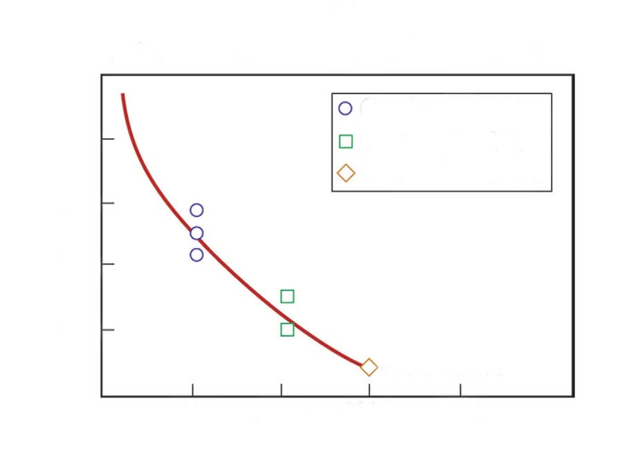
Fig1
The third method uses atmospheric dry plasma etching to remove surface damage.This method offers the advantage that the surface damage is removed, the edges are improved by rounding the sharp edge, and the surface roughness can be controlled where needed for adhesion.
In order to handle delicate thin wafers the device wafer is bonded to a rigid carrier substrate prior to the back-thinning process.The originally thick device wafer is bonded with its active surface to a carrier wafer using an adhesive bonding layer.After backside processing, including the thinning process and eventually further process steps (lithography, etching, etc.), the thin device wafer, supported by the rigid carrier substrate, has to be released from the carrier wafer, enabling dicing and packaging processes in the final stages.
All the necessary processes to create ultra-thin devices are available and only need to be refined. The fragility of the wafer structure before singulation demands special procedures in order to complete the processing.After the wafer has been singulated into chips, the problems of fragility diminish.The development of throughhole interconnect and chip stack, be it in chip or wafer form, brings the back end process into the fab.This implies greater process control from start to finish. Back-end processing has always been considered as outside the fab environment. Bringing it inside will only benefit the final device reliability.
上一篇: 用于高性能硅光子电路的浸没式光刻
下一篇: GaN/GaAs半导体结构的电学性能