The samples reported here were grown in two identical vacuum-connected Perkin Elmer 430 molecular beam epitaxy (MBE) systems. One system was modified to permit the addition of a Wavemat MPDR electron cyclotron resonance plasma source which was used to provide a flux of ionized and atomic nitrogen. Nitrogen was taken from liquid-nitrogen boil-off, filtered first ,for particulates and finally for impurities using a Semigas Nanochem titer. While GaN was being deposited, excess nitrogen was pumped by a diffusion pump which used low vapor pressure Fomblin oil and several stages of cryobaffles to prevent any contamination of the epitaxial layer. For GaAs growth, the MBE was pumped using standard cryoshrouding, ion and cryopumps.
The layer structure shown in Fig. 1 was a initiated in a standard manner by desorbing the oxide from a semi-insulating (lOO)GaAs substrate and subsequently depositing a GaAs buffer layer and collector structure. To initiate the GaN growth, the Ga shutter was closed while the sample remained at 580 “C under an As flux. Once the nitrogen plasma was successfully lit, the Ga shutter was opened and the As shutter was closed simultaneously. GaN was grown at a rate of 500 A per hour at approximately 620 “C! until the desired thickness was obtained under a nitrogen over pressure of approximately 1 x 10 -4 Torr. The GaN was determined by in situ high-energy electron diffraction to be roughly cubic with approximate lattice constant of 4.5 A. After pumpdown, the sample was transferred under ultrahigh vacuum conditions to the second MBE in which the GaAs emitter was grown.
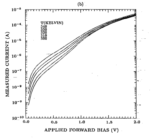
The experimental IV curves in the temperature range 340 down to 300 K are shown in Fig. 2. Figure 2 (a) shows the currents with a negative bias applied to the emitter, while Fig. 2(b) shows the currents with a positive bias applied to the emitter. Below 300 K the reverse bias curlation band bending in the emitter of Fig. 1 (a). The accumulation band bending puils down the barrier top with respect to the Fermi level thereby decreasing the effective barrier height to electron current. Second, the triangular top of the barrier is less effective as an insulator because eleotionscan more easily tunnel through this thin part of the barrier. Both of these factors lead to large forward bias currents.

Fig2(b)
This research is supported by the Office for Naval Research contract No. NOOO14-89-J-1780 and monitored by M. Yoder. The authors would like to thank G. Demaggio of Wavemat Inc. and B. Bowdish of the University of Illi-. nois for their tireless technical support, and Dr. C. W. Litton of Wright-Patterson AFB for his interest. We also wish to thank M. Yoder for his enthusiasm for and encour agement of this effort. One of us (S.S.) wishes to acknowledge the support of a NSF Graduate Fellowship and an AFOSR Graduate Fellowship during different stages of this research.
上一篇: 超薄半导体晶圆应用及工艺