We report on AlGaN/GaN metal–oxide–semiconductor heterostructure fifield-effect transistors (MOS-HFETs)grown over insulating 4H–SiC substrates. We demonstrate that the dc and microwave performance of the MOS-HFETs is superior to that of conventional AlGaN/GaN HFETs, which points to the high quality of SiO2 /AlGaN heterointerface. The MOS-HFETs could operate at positive gate biases as high as 1 10 V that doubles the channel current as compared to conventional AlGaN/GaN HFETs of a similar design. The gate leakage current was more than six orders of magnitude smaller than that for the conventional AlGaN/GaN HFETs. The MOS-HFETs exhibited stable operation at elevated temperatures up to 300 °C with excellent pinch-off characteristics. These results clearly establish the potential of using AlGaN/GaN MOS-HFET approach for high power microwave and switching devices.
The built-in channel of our MOSHFET is formed by the high density 2D electron gas at the AlGaN/GaN interface as in regular AlGaN/GaN HFETs. However, in contrast to HFETs the metallic gate is isolated from AlGaN barrier layer by a thin SiO2 fifilm. Thus the MOSHFET gate behaves more like a MOS structure rather than a Schottky barrier used in regular HFETs. Since the properly designed AlGaN barrier layer is fully depleted by electron transfer to the adjacent GaN layer, the gate insulator in MOSHFET consists of two sequential layers: SiO2 fifilm and AlGaN epilayer. This double layer insulator provides extremely low gate leakage current and allows for a large negative to positive gate voltage swing. Due to the wide band gap and to the full depletion of the AlGaN barrier neither electron nor hole parasitic channel forms at SiO2 – AlGaN interface at the gate voltages up to 1 10 V. The absence of the parasitic channel is confifirmed by our simulations and by the measured capacitance–voltage (C–V) and current–voltage (I –V) characteristics discussed below.
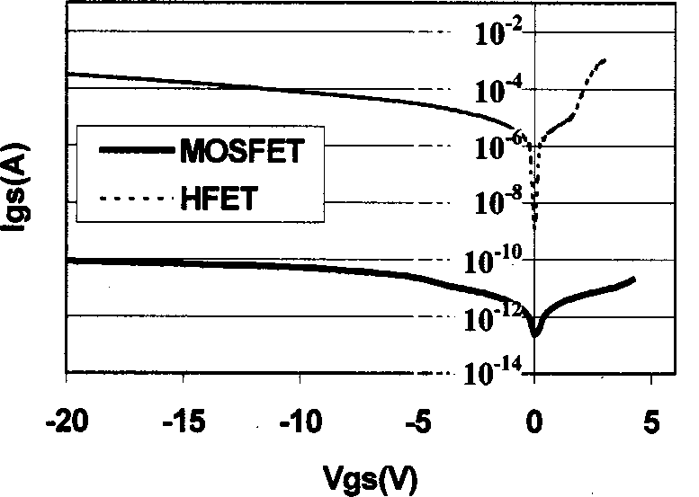
In Fig. 4, we show the gate leakage current for the two device types with an identical geometry(2 μm3x200μm gate area) . The data shows that at room temperature the MOSHFET leakage current is as low as 100 pA at 2 20 V gate bias and is approximately six orders of magnitude smaller than for the HFET with similar gate dimensions. The pinch-off characteristics of AlGaN/GaN MOSHFET were measured in the temperature range 25–300 °C. The pinch-off current as low as 0.15 nA/mm at room temperature and 38 m A/mm at 250 °C was measured at the gate voltage Vg 52 15 V and the drain bias of 10 V. Even at temperatures as high as 300 °C the pinch-off current remains approximately 10 mA/mm, which is about two orders of magnitude less than the maximum saturation current. No degradation was observed in the maximum saturation current up to 300 °C. The results of Figs. 3 and 4 clearly establish the potential of using our MOSHFET devices for high voltage, high temperature applications.

Fig4
In conclusion, we demonstrated high performance SiO2 /AlGaN/GaN/SiC MOSHFETs with stable operation at elevated temperatures up to 300 °C. The measured dc, rf, rf power, and high temperature characteristics of the MOSHFET are equal to or better than for identical geometry HFET devices. This clearly establishes the feasibility of the AlGaN/GaN MOSHFET device approach for highfrequency, high-temperature, high-speed switching applications.
上一篇: GaN/GaAs半导体结构的电学性能
下一篇: 具有宽带隙GaN半导体的硅上集成光子学