We present the fabrication and characterization of nonintentionally doped GaN and GaN:Mg Schottky metal–semiconductor–metal (MSM )photodetectors, grown on sapphire by metalorganic chemical vapor deposition. Low-leakage, Schottky contacts were made with Pt/Au. The devices are visible blind, with an ultraviolet/green contrast of about fifive orders of magnitude. The response times of the MSM devices were , 10 ns and about 200 ns for GaN and GaN:Mg, respectively. The noise power spectral density remains below the background level of the system (102 24 A2 /Hz) up to 5 V, for the undoped GaN MSM detector.
Gallium nitride has been the focus of intense interest in recent years due to advances in crystal growth technology and device fabrication procedures. Its direct, wide band gap makes it an ideal choice for use in various detector applications such as ultraviolet (UV) astronomy, flflame detection, and engine monitoring, where harsh working environments exploit the natural durability and visible blindness of the material.
A Xe arc lamp was used as the optical source for the spectral responsivity studies and a standard synchronous detection scheme was employed to measure the front-side illuminated detector signal. The system was calibrated with an UV-enhanced Si detector. The responsivity dependence on optical power was determined by excitation with a continuous wave He–Cd laser ( 325 nm). The response time of the detectors was measured using a pulsed nitrogen laser ( 337 nm) as the optical source. Noise characterization was performed using a SR760 fast Fourier transform spectrum analyzer with the devices connected to a Keithley 428 current amplififier, so that the background noise power density of the system is about 102 24 A2 /Hz.

Fig3
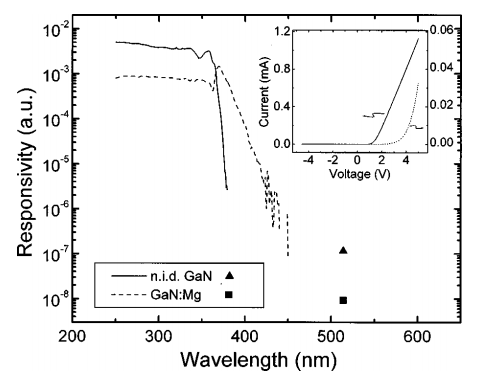
MSM detectors are shown in Fig. 2. The most striking difference between these two response curves is the slope of the wavelength cutoff. The response of the GaN MSM detector shows a very abrupt cutoff, whereas the GaN:Mg MSM detector has a more gradual decline at longer wavelengths. This slight absorption of photons with energy below the band gap is due to the presence of Mg related levels in the material. Using the measurement setup described above, it was not possible to detect any photogenerated signal for wavelengths longer than 400 nm. Therefore, an Ar laser (514 nm) was used to obtain a photoresponse in the visible spectral region, also displayed in Fig. 2. Both response curves exhibit high visible rejection, with an ultraviolet/green contrast of about fifive orders of magnitude.
The photocurrent increases linearly with the optical power for the GaN:Mg device as seen in Fig. 3, and shows no saturation at higher power levels. The nid GaN device, however, follows a Pk fifit, where P is the optical power and k5 0.9, which is a much better result than the k5 0.1 behavior reported for nid GaN photoconductors.3 To investigate the possibility of an internal gain mechanism, the responsivity was measured with respect to the voltage bias. The results of this test are seen in the inset of Fig. 3. Both the nid GaN and the GaN:Mg MSM devices exhibited a scaling of the responsivity with voltage bias. This increase indicates the presence of an internal gain mechanism such as hole trapping. The shape of the spectral response has been found to be independent of bias up to 5 V.