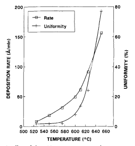
Low pressure chemically vapor deposited polysilicon deposition was studied from 525 to 650℃ The silicon appears to be amorphous with a smooth surface up to 550℃ and completely crystalline above 600℃ The transition region is found to be from 560 to 590℃ This transition is marked by sharp crystallographic and resistivity changes. The smooth surface morphology of the amorphous silicon is found to be preserved after POC13 doping and a 1000℃ oxidation. The preservation of this smooth morphology is demonstrated to be due to the presence of a native oxide on the surface of the silicon upon exposure to atmosphere. However, an in situ anneal of amorphous silicon at 610℃ results in large coarse crystals with rough surface morphology and disparate orientation. The smooth morphology of the 550℃ silicon is found to be transmitted through subsequent polycide structure layers. The impact on device reliability is discussed. The amorphous silicon is found to have a higher plasma etch rate than the polysilicon.
Doped polysilicon is widely used in very large scale integrated (VLSI) device fabrication as gate electrodes, interconnect material, and as resistors in static memory circuits. As gate electrodes, the surface morphology is an important factor in device reliability, as the presence of asperities on the film surface can lead to premature device failures from localized high electric fields. Thus it is highly desirable to have gate electrodes with smooth surfaces. 1-6 Where device speeds of 100 μs or less are required, the faster access times require even lower resistivity than can be realized with doped polysilicon. In this instance, therefore, tungsten silicide is often deposited on the doped polysilicon and the polycide becomes the interconnection material. As polycide etching is anisotropic, polycides with rough morphologies require extended overetch to remove highlight residues. This extended etching may have a propensity for the pitting of the substrate which would degrade device reliability. Consequently, polycides with smooth morphologies would be preferred.
The most common technique for silicon deposition is in its crystalline form by tow pressure chemical vapor deposition (LPCVD) from Sill4 at temperatures above 600℃ In this sequence, in single gas inlet reactors, the deposition rate is such that the silane is depleted down the furnace and the deposition rate decreases accordingly. To compensate for this drop in deposition rate, a temperature gradient is often used, the temperature setpoints being ramped along the length of the furnace from the injection points. The drop in deposition rate from the silane depletion is, thereby, compensated for by the increase in deposition rate from the higher temperature. With this approach, while there is uniformity in thickness, the microstructure of the films being a function of the deposition temperature, would vary across the reactor. The films would exhibit different properties: optical, morphological, doping, and microstructural depending on the location in the reactor. The polysilicon dependent device properties may also vary accordingly. In its crystalline state, polysilicon has a rough surface morphology. However, it is reported that a smooth morphology may be obtained if the film is deposited amorphously and subsequently annealed at a higher temperature. Kamins attributed this preservation of the smooth morphology to the presence of a native oxide on the surface of the silicon film. Hendricks and Mavero proposed an alternative model. They suggested that the surface smoothness is preserved because grain growth during annealing involves relatively small atomic distances whereas surface roughness requires distances which are large compared to interatomic distances. The exact mechanism, however, has not been established by experimentation. It is, however, important that this mechanism be established.

Fig1
The surface morphology of the polysilicon and the polycide was evaluated with a JEOL field emission scanning electron microscopy (SEM). The degree of surface roughness was also monitored by measuring the transmittance of the film at 200 nm with a Hewlett-Packard UV spectrophotometer.
A two-step deposition was used to explore the mechanism by which the smooth surface morphology of the amorphous silicon is preserved after a high temperature cycle. The first step was at 550℃ for a thickness of 1500 A, and the second at 610℃ for 800 A. One sequence was done in situ and the other was separated with the wafers exposed to the atmosphere between depositions. Both films were POCI3 doped and secondary ion mass sepectroscopy (SIMS), TEM, and SEM analyses performed.
上一篇: InP光子学与硅电子学的集成
下一篇: 用于自旋电子学的宽带隙GaN基半导体