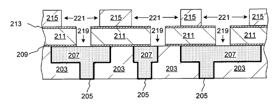
Methods for removing silicon nitride and elemental silicon during contact preclean process involve converting these materials to materials that are more readily etched by fluo ride-based etching methods, and Subsequently removing the converted materials by a fluoride-based etch. Specifically, silicon nitride and elemental silicon may be treated with an oxidizing agent, e.g., with an oxygen-containing gas in a plasma, or with O. or Os in the absence of plasma to produce a material that is more rich in Si-O bonds and is more easily etched with a fluoride-based etch. Alternatively, silicon nitride or elemental silicon may be doped with a number of doping elements, e.g., hydrogen, to form materials which are more easily etched by fluoride based etches. The methods are particularly useful for pre-cleaning contact vias residing in a layer of silicon oxide based material because they minimize the unwanted increase of critical dimension of contact vias.
This application claims priority under 35 USC 119(e) from U.S. Provisional Patent Application No. 60/905,782 naming Liu et al. as inventors, titled “Methods of Removing Silicon Nitride and Other Materials during Fabrication of Contacts and Interconnects' filed Mar. 7, 2007, which is herein incor porated by reference in its entirety and for all purposes. This application is related to U.S. patent application Ser. No. 1 1/479,812 filed Jun. 30, 2006, naming Liu et al. as inventors, titled Adsorption Based Material Removal Process', which is incorporated herein by reference in its entirety and for all purposes. This application is also related to U.S. patent appli cation Ser. No. 12/002,085 filed Dec. 13, 2007, naming Liu et al. as inventors, titled “Modulating Etch Selectivity and Etch Rate of Silicon Nitride thin Films', which is incorporated herein by reference in its entirety and for all purposes.
The present invention pertains to methods of removing layers of material on a partially fabricated integrated circuit. Specifically, the invention pertains to methods for removing silicon nitride and other materials during fabrication of con tacts and interconnects.
In a typical integrated circuit manufacturing process flow, metal is deposited onto a patterned dielectric (typically a 35 silicon dioxide based material) to fill the vias and trenches formed in the dielectric layer. The resulting metallization layer is typically formed either directly on a layer carrying active devices (e.g., transistors), or on another metallization layer. The resulting metal-filled vias and trenches form the 40 conductive pathways of an integrated circuit (IC) device. Contacts and interconnects are formed between active devices and metal-filled vias as well as between metal lines of adjacent metallization layers.

Fig1
Removal of silicon nitride presents several challenges, which become more pronounced as the dimensions of recessed features in IC devices continue to shrink. Silicon nitride is often more resistant to fluoride-based etching than the surrounding silicon dioxide based ILD, and therefore often requires more aggressive etching conditions. Removal of even very small amounts of etch-resistant silicon nitride from the contacts and interconnects, can inadvertently result in etching of Substantial amounts of silicon dioxide based ILD material, which defines the dimensions of recessed fea tures on a partially fabricated IC device. While such inadvert ent etching may be tolerated in Some device structures with relatively large dimensions of recesses, in those structures where dimensions are small, fluoride-based etching of etch resistant silicon nitride may lead to Substantial increase in critical dimensions of vias and trenches defining the contacts. Such increase in critical dimensions is highly undesired, and should be avoided when possible.
上一篇: 光致抗蚀剂底层成膜组合物和图案形成方法
下一篇: 最终冲洗期间晶片表面的原生氧化物生长