We have achieved uniform etched depth regardless of feature size by employing a combination of anisotropic plasma etching in Ž . inductively coupled plasma ICP followed by wet etching. In our approach, the original feature is divided into small elementary features in a mosaic-like pattern. These individual small features are all the same size and thus exhibit identical etch rates and sidewall profiles. Final patterns are completed by wet etching: the ridges between the elementary features are removed in TMAH. In this paper, we present the results obtained using this dryrwet etching sequence. The benefits and limitations of this method are described. Extensions to more complex multidepth structures are discussed.
Plasma etching of deep structures is difficult because the etch rate depends on feature size and, through etch time, on the aspect ratio. These phenomena are often Ž described using the terms reactive ion etch lag RIE lag, . small features etch slower than large features and aspect Ž . ratio-dependent etch rate ARDE . Even though RIE lag was historically first observed in submicron integrated circuit fabrication, it is not specifically a submicron phenomenon: it has been observed in MEMS structures with linewidths of tens of micrometers as well. RIE lag and ARDE are manifestations of limited transport of etchants w x into high aspect ratio structures. RIE lag can be minimized in certain process conditions, but it is usually unavoidable with high etch rate recipes. An extreme example of pattern size effect in inductively coupled plasma Ž . ICP etching is shown in Fig. 1.
Another important source of depth non-uniformity is the loading effect. Large exposed areas cause slowdown of etch rate and can adversely affect the radial uniformity.
The etch depths were measured from sawn cross-sec- Ž . tions with scanning electron microscope SEM . The resulting surface roughness was measured with an atomic Ž . force microscope AFM . The ICP etch process used for the AFM sample preparation was the low rate one for 90 min and large 2x2 mm patterns to achieve a practical sidewall height and bottom area for measurement.
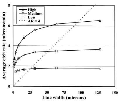
Typical etch result of our process for a traditional multiwidth structure is shown in a SEM micrograph in Fig. 1. The medium rate process has an extremely high selectivity against oxide mask and the aspect ratio dependence is moderate for relatively wide trenches. The low rate plasma etch process has slightly positive profile and the medium rate process has almost vertical slightly bowing profile. The etch rates of these processes are plotted as a function of pattern width in Fig. 2. Other main characteristics of these etch processes are published elsewhere. All three processes suffer from a severe loading effect. The results of macroscale loading on the high etch rate process are shown in Fig. 3.

Fig2
Typical results using the medium rate process are shown in Fig. 4. ICP etching results in 25% variation in etch depth between the largest and smallest features. The bottom of the largest feature is convex. With mosaic layout, the etch depth is uniform for all narrow lines. The etch depth in this case is 100 μm.
Uniform depth, regardless of pattern width, can be achieved using a combination of dry and wet etching methods. Pattern size and depth control using the dryrwet etching sequence described here is better than in traditional plasma etching. Multidepth structures defined by a single lithography step can be fabricated using an extension of this method.