Chip scale package (CSP) is defifined as the package that has an area of less than 1.2 times of die size. Due to its smaller form factor, CSP is more applicable for handheld devices. As for wafer level CSP (WLCSP or WLP), the package has the same size as die size, and full package fabrication processes are implemented at wafer level. One of the biggest advantages of WLCSP lies in its cost saving. As the entire wafer is tested and packaged at wafer level, the processing cost almost remains the same with the increasing number of dies per wafer. Also, there is no material waste in wafer level molding compared to traditional transfer molding.
WLP can be categorized into fan-in and fan-out WLP. As shown in Fig. 1, fan-in WLP (the standard WLP) has the same size as the die, and fan-out WLP extends its size by a fan-out area. As for fan-in WLP, the package I/O number is limited due to the small die size, and fan-out WLP somehow improves the ball number by extending a redistribution layer (RDL) to fan-out areas. Both of them adopt a redistribution technology to realize the interconnection between the die and solder balls, so mostly there is the RDL between chips and solder balls. For different companies, the redistribution process may differ signifificantly.
This paper reviews the advances of wafer level packaging in recent years. The emerging technology of fan-out WLP and its typical applications are introduced fifirst. A brief review on threedimensional (3D) integration with WLP technology is presented. Reliability problems faced with fan-in, fan-out WLPs, and 3D packaging are presented, and methods of improving reliability are also discussed in the last part.
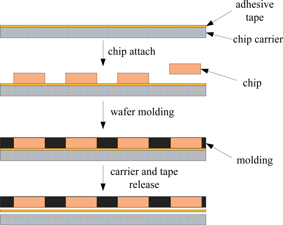
One of the main differences between traditional packages and WLPs lies in the fabrication process. As for traditional IC packages, the wafer is fifirstly cut into small dies, and all the packaging processes are implemented on the single die. With the increasing of die numbers, more equipment and labors are needed. WLPs adopt the batch process and all the packaging processes are realized on the entire wafer. One of the advantages of the batch process is that the packaging cost will not increase with the increasing of die numbers.

Fig1
Reliability enhancement could also be realized through bump shape optimization and solder material selection . Analysis on the effect of different bump shapes to solder joint reliability shows that with the same height and pad opening, the larger the bump diameter is, the worse of joint fatigue life performance . Figure 9 shows three scenarios of solder ball shapes. The large solder ball diameter means more solder volume, which intuitively may provide stronger support for solder ball against fatigue failures. Finite element analysis has been performed on those three scenarios and the results of per-cycle inelastic strain energy density are tabulated in Table 1. It shows that the convex shape solder ball (more solder volume with a larger diameter) will result in the worst solder joint reliability performance.
This work was fifinancially supported by National Science and Technology Major Project of China (Grant No. 2011ZX02601), the Key Natural Science Foundation of the Jiangsu Higher Education Institutions of China (Grant Nos. 10KJA140043 and 08KJA510002), “333 high level talents training project” in Jiangsu province, and the fifirst “Enterprise Doctor Concentration Plan” of Jiangsu Province.
下一篇: Er掺杂GaN半导体薄膜的发光特性