This paper presents a comparative study of the impact of metal wet etch on carrier mobility and metal gate/high-k device characteristics and reliability. A TaSiN metal wet etch process that is highly selective to the underlying HfO2 dielectric has been developed. While the metal wet etch slightly degraded the electron mobility, it did not affect hole mobility. It did not show any effect on fast transient charge trapping, and, in fact, improved negative bias temperature instability (NBTI) and positive bias temperature instability (PBTI).
Since PVD deposition of the first metal generally results in a larger damage to the underlying high-k dielectrics than chemical vapor deposition (CVD) or ALD techniques, the results from this experiment would be close to the worst-case scenario. Because both NMOS and PMOS transistors were studied, ALD TiN, which has a mid-gap work function, was chosen as the second metal gate material.
To differentiate the impact of wet chemical exposure from the effects of metal deposition and metal wet etch, TaSiN metal deposition was omitted in another experimental split; however, the HfO2 was exposed to SC1 and NH4OH wet chemicals before the deposition of the ALD TiN metal gate. As a comparison, control TiN/HfO2 CMOS transistors without the metal deposition and wet chemical exposures were also fabricated.
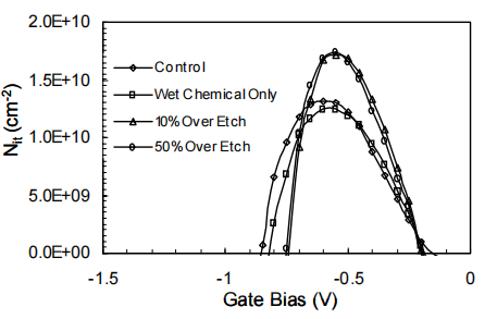
Figure 5 shows the charge pumping results measured on a 10X1 µm NMOSFET. The wet chemical exposure only and the longer over etch time do not increase the interface trap density (Nit); however, the metal deposition and metal wet etch increase the Nit by ~30%. This Nit increase could be related to the TaSiN PVD deposition, which can have a negative effect on the interface trap density.
The within-wafer distributions of the linear Vt of a 10X1 µm NMOSFET and PMOSFET are shown in Figure 3. We can see that the Vt distribution is not degraded by the metal wet etch, indicating a uniform metal wet etch process across the wafer. For the NMOSFET, the metal wet etch resulted in a negligible Vt shift, because the effects of the small negative Vfb shift and the slightly thinner EOT cancel etch other. For the PMOSFET, the metal wet etch led to a ~20 mV reduction in the linear Vt .

Fig5
Figure 6 (a) and (b) show the electron and hole mobility measured by the DC technique. For the NMOSFET, the wet chemical exposure only has only a negligible effect on electron mobility; however, the TaSiN deposition and wet etch degrade both peak mobility and high-field mobility. At Eeff = 1 MV/cm, the high-field electron mobility decreases from 200 cm2 /V-sec for the control device to ~188 cm2 /V-sec for the devices that received the metal wet etch. For PMOSFETs, the effects of the TaSiN deposition and wet etch on hole mobility are negligible. In fact, the device that received wet chemical exposure only shows slightly improved peak hole and high-field hole mobility. The degradation of the electron mobility by metal deposition and metal wet etch processes is coincident with the increased Nit for the devices that received metal wet etch process. Since hole mobility is generally less sensitive to the interface quality than the electron mobility, it is not surprising that the TaSiN metal wet etch does not impact the hole mobility. These results imply that in dual metal gate CMOS fabrication, the n-type metal should be deposited first so that only the PMOS portion will undergo the metal wet etch process.
NBTI-induced Vt instability has also been observed in Hf-based high-k dielectrics [9]. It was found that the NBTI in high-k devices is comparable to that in SiO2 and SiON devices. Since the Hf-based high-k stack always has a SiO2 or SiON bottom interface, it is believed that the same depassivation of the oxide/Si interface and subsequent proton diffusion are responsible for the NBTI in high-k devices .