An apparatus for electroplating a wafer surface includes acup having a central aperture defined by an inner perimeter,a compliant seal adjacent the inner perimeter, contactsadjacent the compliant seal and a cone attached to a rotatablespindle. The compliant scal forms a seal with the perimeterregion of the wafer surface preventing plating solution fromcontaminating the wafer edge, wafer backside and the con-tacts. As a further measure to prevent contamination, theregion behind the compliant seal is pressurized. By rotatingthe wafer during electroplating, bubble entrapment on thewafer surface is prevented, Further, the contacts can bearranged into banks of contacts and the resistivity betweenbanks can be tested to detect poor electrical connectionsbetween the contacts and the wafer surfacc.
The manufacture of semiconductor devices requires theformation of electrical conductors on semiconductor wafers.For example, electrically conductive leads on the wafer areoften formed by electroplating (depositing) an electricallyconductive material such as copper on the wafer and intopatterned trenches.
Brogden et al,U.S. Pat. No. 5,227,041 (hereinafterBrogden),teaches a dry contact electroplating apparatuswhercin a number of electrical contacts are provided adja-cent to a central aperture of a base of the apparatus. Brogdenfurther teaches that the contacts preferably includerelatively-sharp tips for piercing any insulating substanccwhich may be present on the wafer plating surface.However, even with relatively sharp tips, one or more of thecontacts may form a poor electrical connection with thewafer plating surface. This results in nonuniformity of thedeposited electrically conductive layer. To determine if oneor more poor electrical conneetions were made with thewafer plating surface, the wafer can be-tested to measure theuniformity of the deposited electrically conductive layer.However, wafers exhibiting nonuniformity of the depositedelectrically conductive layer must be discarded reducing theyield of the electroplated wafers. Further, it is not practicalor cost effective to test every wafer. Thus, it is desirable tobave an apparatus for electroplating a wafer which providesuniform electrical contact with the wafer plating surfacewhile at the same time providing a means of readily testingthe intcgrity of the electrical contact with the wafer platingsurface before the wafer is electroplated.

Fig1
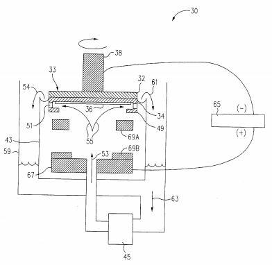
FIG. 1 is a diagrammatical view of an electroplating apparatus having a wafer mounted therein in accordance with the present invention.
The rotary union has a lower connector or a lowerconnector in combination with a tube connector whichallows the pressure/vacuum passage to be coupled to aninner coaxial tube and the pressure passage to be coupled toan outer coaxial tube. Of importance, this allows bothvacuum and pressure to be provided through the inner andouter coaxial tubes, respectively, to a rotating clamshell ofthe electroplating apparatus. Since the inner and outercoaxial tubes sharc a common axis (the inner tube beinginside of the outer tube), the space required for the tubing isreduced to that of the outer coaxial tube compared to havingboth the inner and outer tubes in a side by side arrangement.This is particularly advantageous for use in an electroplatingapparatus in accordance with the present invention whereinsize constraints of the pressure and vacuum lines, as well asconcentric geometry, require coaxial tubing of the pressureand vacuum lines.
上一篇: Er掺杂GaN半导体薄膜的发光特性
下一篇: 低温深反应离子蚀刻中掩模材料的影响