Cryogenic silicon etching in inductively coupled SF6 /O2 plasma has been studied, especially the behavior of mask materials. Suitability of eight different mask materials for cryogenic silicon deep reactive ion etching has been investigated. Three of the fifive photoresists suffered from cracking during cryogenic etching. We clarifified the stages of the etching process and identifified two mechanisms behind the cracking: thermal expansion mismatch and mechanical deformation from wafer clamping and backside helium pressure. Also thickness of the photoresist plays a role in cracking, but, contrary to common conception that all thick resists suffer from cracking in cryogenic etching, we found that SU-8 negative resist did not crack, even for very thick layers. This is explained to be due to its high cross-linking density. All three hard mask materials had high selectivities and were free of cracking problems. However, aluminum mask resulted in poor surface quality, while thermally grown SiO2 and amorphous Al2O3 deposited by atomic layer deposition showed smooth surfaces and sidewalls. Silicon dioxide had selectivity of 150:1, while Al2O3 selectivity was 66 000:1. This extreme selectivity of Al2O3 mask, combined with good surface quality, is shown to be highly benefificial in both shallow and through-wafer etching.
Cryogenic deep reactive ion etching (DRIE) of silicon was fifirst introduced by Tachi et al. in 1988.They observed that etch rate and selectivity increased at cryogenic temperatures but more importantly, the anisotropy of etching improved remarkably. Nowadays cryo-DRIE is commonly utilized in fabrication of microelectromechanical systems because of its ability to produce high-aspect-ratio structures at high etch rates >5 μm/min . The biggest advantage of cryo-DRIE over the pulsed Bosch process4 is sidewall smoothness.
Selection of the etch mask material is an important issue. The etch rate of the mask must be low, but its application and patterning should be easy. The most natural mask material is photoresist, but selectivity of photoresists is usually poor compared to hard masks and therefore deep etching may not be possible with photoresist masks.5 In cryogenic DRIE, the other major downside of the photoresists is their vulnerability to cracking. Thin photoresists (<1.5μm) are reported to be free of problems but thicker resists are prone to cracking. Plasma damage to resists exposed to temperatures in excess of glass transition temperature (Tg) is known to inflflict problems,but photoresist cracking at cryogenic temperatures has not been given attention before. Mask material selection may also affect etch rate, undercutting, and surface quality of the etched features.

Fig1
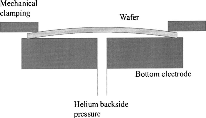
The results presented in Table V strongly suggest that the wafer deformation caused by the helium backside cooling also plays a role in photoresist cracking at low temperatures. It must be emphasized that wafer deformation caused by helium cooling system by itself is not enough to cause photoresist cracking, but it is evidently one mechanism that can initiate cracking at cryogenic temperatures. It was also noticed that AZ 5214 E photoresist cracks easier if the etching is done immediately after lithography, which is probably because of larger temperature gradient.
When using AZ 1505 photoresist mask, all etched surfaces are smooth, but low selectivity and thin mask layer thickness limit its use to shallow etchings. Thicker AZ photoresist layers are prone to cracking. In our experiments, the only thick photoresist that did not crack at cryogenic temperatures was SU-8. Therefore selectivity does not limit the etch depth, but troublesome removal of SU-8 narrows down the practical applications of SU-8 as an etch mask. Surface quality of etched silicon is good when using SU-8 mask (Fig. 6)if mask layer is not extremely thick. Sidewall roughness might become a problem when using 60 μm thick SU-8 mask.
The behavior of the eight different mask materials during cryogenic DRIE was studied. Three of the fifive photoresists used suffered from cracking. AZ 1505 and SU-8 of any thickness were not vulnerable to cracking in our experiments. Thin resists are known to be suitable for cryogenic etching, but remarkable result was that SU-8 layers at least up to 60 μm were also suitable for cryogenic processing. The experimental results suggest this to be due to the exceptionally high cross-linking density of SU-8.
上一篇: 半导体晶片上电镀铜的方法
下一篇: 单晶硅的完整 3D蚀刻轮廓分析