Purpose The life cycle assessment of silicon wafer processing for microelectronic chips and solar cells aims to provide current and comprehensive data. In view of the very fast market developments, for solar cell fabrication the influence of technology and capacity variations on the overall environmental impact was also investigated and the data were compared with the widely used ecoinvent data. Methods Existing material flow models for silicon wafer processing for microelectronic chips and solar cells used for engineering and planning formed a starting point for this analysis. The models represent an average of widely used processes and associated process equipment. The resulting input/output tables formed the data basis for the life cycle assessment. This is a cradle-to-gate investigation, consisting of primary gate-to-gate data for wafer processing. The upstream processes of the necessary inputs were supplemented with data from ecoinvent v2.0. Subsequent manufacturing steps, utilization, and waste disposal of the final products were not included. The software used for creating the inventory and impact assessment was Umberto version 5.5. The Impact 2002+ method was applied for impact assessment.
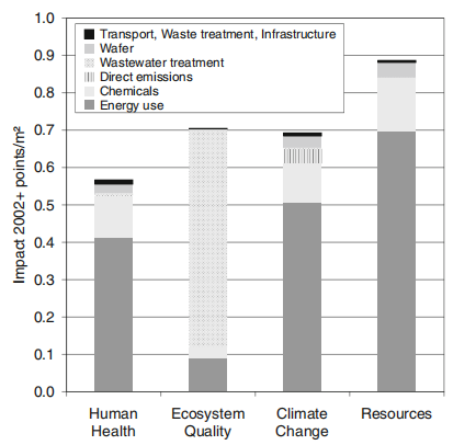
Results For both semiconductor and solar cell fabrication, energy consumption and upstream chemicals production are most relevant for the overall potential environmental impact when only the gate-to-gate processes are considered. The upstream process for wafer production is dominant in solar cell fabrication, but exerts little influence on semiconductor fabrication. In the case of semiconductor fabrication, a comparison with the present ecoinvent dataset “wafer, fabricated, for integrated circuit, at plant” shows large differences. Conclusions In the case of silicon solar cells, the results of this study and the ecoinvent data are very similar and the impact of different fabrication processes appears to be minor.
Processing crystalline silicon and using the semiconducting effect form the basis of both industries. Processes of semiconductor fabrication are also found in solar cell fabrication, although processing microelectronic wafers is more precise. In crystalline silicon solar cell production typically five to seven process steps are applied in a linear sequence to the bare wafer, before the processed wafer is cut and used to build-up photovoltaic modules. Whereas in microchip fabrication there are up to 400 process steps before the array of microchips on the silicon wafer is finished and can be cut, packaged, and bound to electrical connections. These 400 process steps are run in about 12 specialized process areas, which require the wafer to circulate in the area of production. The different structure of production results also in very different times required to complete production (“cycle time”).

Fig1
One reason for the higher values of ecoinvent data by comparison with DRAM wafer production according to M +W Germany data is the assumption for the yield. ecoinvent takes a value of 55%, which represents the average of several widely ranged literature values. This value is unrealistic in current practice and as an average, since at such a low yield the process cannot be operated economically.
The low yield is not solely responsible for the differences. Figure 4 shows the results broken down by their contributions. Waste treatment and energy consumption show the biggest differences, at least for DRAM fabrication.
Other differences exist in the data on energy consumption for the wafer processing. The energy consumption for both datasets is composed of electricity and natural gas, the quantity is shown in Table 11. Natural gas consumption especially is 30 to 80 times higher for ecoinvent compared to this study. As ecoinvent assumes the same energy demand for memory and logic wafer fabrication, the quantity for logic wafer seems to be accurate. However, the underlying literature source for ecoinvent refers only to DRAM fabrication, for which the quantity of nearly 100,000 MJ is almost three times higher than M+W Germany data.
A reason for the high-energy consumption in ecoinvent seems to be a lack of data, since only two literary sources were cited. As technology is developing rapidly in semiconductor fabrication, swift improvements in energy efficiency in this field can be expected too, so that the data quickly become outdated.
上一篇: 多晶硅材料中金属杂质的化学性质及其分布
下一篇: 快速热化学气相沉积设备中硅片的热分布评估