Organic light emitting diode devices (OLED) have potential applications in flat panel displays, flexible displays and illumination devices. In this paper the effect of a photonic crystal structure in the glass substrate on the emission characteristics is investigated by means of FDTD simulations.
In this paper a photonic crystal structure (PC) based on air holes in a glass substrate is designed. It has a TE band gap but TM waves do not have a forbidden band. By a 3D FDTD simulation using periodic boundary condition (PBC), this structure was excited by a dipole in the center of the structure at the interface of the hole transport layer (HTL) and the electron transport layer (ETL). The near-field out-coupled light is recorded for the case with and the case without photonic crystal. It is shown that for the structure with photonic crystal the light emission in OLED is suppressed.
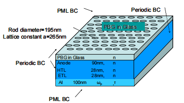
The geometry of the photonic crystal enhanced OLED has been illustrated in figure.3. The structure is excited by a sinusoidal electric dipole at the HTL/ETL interface, with frequency corresponding to a wavelength λ=530nm for 4096 time steps (equivalent to about 32 periods). The dielectric parameters are given in Table 1.
The simulation volume is X=250×dx, Y=250×dy where dx=dy=dz=λ/32. dt=dx/4/c. The periodic boundary condition (PBC) is used for the four sides of the volume and the perfectly matched layer (PML) boundary condition for top and bottom . The structure is analyzed with photonic crystal and without photonic crystal. The near-field plot of the z component of poynting vector in the OLED without photonic crystal is shown in figure. 4a. In figure. 4b the near-field plot of the z component of poynting vector is shown for the structure with photonic crystal.
It is obvious that in one period of oscillation more energy is confined near the location of the dipole in the photonic crystal enhanced OLED (Figure. 5). The ratio of the extracted energy of enhanced OLED over the simple OLED is illustrated in figure 6 as a function of the radial distance from the dipole.

Fig5
Optical extraction of a photonic band gap enhanced OLED was simulated by 3D FDTD method. The metallic layer is modeled as a dispersive material. It is shown that photonic band gap enhancement confines the near-field emission and increases the contrast of the OLED.
上一篇: 不同层对OLED性能的影响
下一篇: 单层和双层石墨烯大单晶的化学气相沉积生长