The growth of large-domain single crystalline graphene with the controllable number of layers is of central importance for large-scale integration of graphene devices. Here we report a new pathway to greatly reduce the graphene nucleation density from B106 to 4 nuclei cm-2, enabling the growth of giant single crystals of monolayer graphene with a lateral size up to 5 mm and Bernal-stacked bilayer graphene with the lateral size up to 300 mm, both the largest reported to date. The formation of the giant graphene single crystals eliminates the grain boundary scattering to ensure excellent device-to-device uniformity and remarkable electronic properties with the expected quantum Hall effect and the highest carrier mobility up to 16,000 cm2V-1 s -1 . The availability of the ultra large graphene single crystals can allow for high-yield fabrication of integrated graphene devices, paving a pathway to scalable electronic and photonic devices based on graphene materials.
Graphene has emerged as an exciting, atomically thin twodimensional material for fundamental studies and potential applications in future electronics. The pristine graphene can be obtained through a mechanical exfoliation approach to break the weak van der Waals forces between the adjacent layers of graphite9. This approach can produce the bestquality graphene, but often with sizes limited in a few to a few tens of micrometres. On the other hand, large-area mono- or few-layer graphene can now be readily obtained through a carbon segregation process on carbon-containing substrates (for example, SiC) or chemical vapour deposition (CVD) process on metal foils (for example, Ni or Cu). In particular, the CVD approach can be used to produce continuous mono- or few-layer graphene with the sizes measured by square metres, but typically with a polycrystalline structure and a high density of domain/grain boundaries, leading to highly variable electronic properties. Even though it has been reported that mobility of the CVD graphene within single domain can be comparable to the best-reported exfoliated sample, the overall transport characteristics of wafer-scale CVD graphene is still largely limited by the crystal defects at domain boundaries. Therefore, to produce large graphene single crystals represents a central challenge for the large-scale integration of functional electronic and optoelectronic devices from graphene.
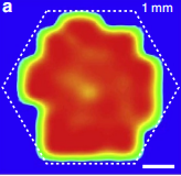
We have conducted transmission electron microscopy (TEM) and electron diffraction studies to confifirm the single crystalline nature of the large hexagonal graphene domains. To this end, the as-grown graphene fifilms were transferred onto an amorphous carbon-covered TEM grid (with 100x100-μm-sized square holes). An SEM image of the graphene on TEM grid shows that a 1.5-mm graphene domain retains its structural integrity with the hexagonal shape well preserved (Fig. 2a). Figure 2b shows a bright-fifield TEM image of the graphene membrane at the edge region (highlighted by a red arrow in Fig. 2a). The graphene membrane is clean, uniform, and the edge is straight.

Fig2a
To evaluate the overall quality of the continuous graphene fifilm made of large-domain graphene, we have also compared the sheet resistances of the continuous graphene fifilms formed by large domains (domain size of B2 mm) and small domains (domain size of B50 mm). To make more fair comparison between largedomain and small-domain devices, we took sheet resistance measurement on multidomain large-area sample (1 cm x 1 cm) so that the transport in both samples need to go across multiple domain boundaries. Here both large (B2 mm domain size) and small (B50 mm of lateral domain size) domain samples are polydomains, where large-domain sample has B20–30 domains and small-domain sample has B40,000 domains. Our studies clearly show that the overall sheet resistance of the large-domain sample is only about one quarter of that of the smaller domain samples (Supplementary Fig. S11), which can be largely attributed to the greatly reduced domain boundary scattering in largedomain graphene fifilm.
In summary, we have shown that the nucleation density of graphene domains in a CVD process can be dramatically reduced from B106 to 4 nuclei cm-2, using an integrated strategy of low reactor pressure, high hydrogen/methane molar ratio and preannealing of the copper foil in pure argon environment, and therefore enabling a straightforward way to prepare the largest single crystals of monolayer and bilayer graphene. The formation of ultra-large single crystalline graphene can enable excellent device performance with highly uniform electrical characteristics. It can therefore pave an effective pathway to large-scale integration of graphene devices with high yield and high reproducibility, which are the key to practical applications.
上一篇: 光子晶体增强型OLED的FDTD模拟
下一篇: 单晶超声波测量