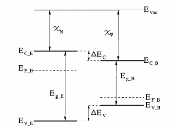
The radiation effects in Ill-V heterojunction devices are investigated in this thesis. Two types of heterojunction devices studied are InGaP/GaAs single heterojunction bipolar transistors (SHBTs) and GaN-based heterojunction light emitting diodes (LEDs). InGaP/GaAS HBTs are investigated for high energy (67 and 105 MeV) proton irradiation effects while GaN heterojunction LEDs are studied for neutron irradiation effects. A compact model and the parameter extraction procedures for HBTs are developed, and hence the 1c VCE characteristics of pre- and post-irradiation HBTs can be simulated by employing the developed model.
GaN heterojunction LEDs are electrically and optically characterized before and after neutron irradiation. Neutron irradiation causes changes in both the I-V characteristic and the light output. Atomic displacement is responsible for both electrical and optical degradation. Both electrical and optical properties degrade steadily with neutron fluence producing severe degradation after the highest fluence neutron irradiation. The light output degrades by more than 99% after 1.6 x10¹⁵ n/cm2 neutron irradiation, and the radiation damage depends on the operating current and is generally less at higher currents.
There are a variety of radiation sources and environments to which electronic systems may be exposed. The one of most interest is space radiation. Radiation in the space environment mainly comes from three categories: (1) the trapped particle belts (2) solar particle events and (3) cosmic rays. The radiation belts (Van Allen belt) consist primarily of electrons of up to a few MeV energy and protons of up to several hundred MeV energy. They are trapped in the Earth's magnetic field; their motion in the magnetic field consists of a gyration about the field lines, a bouncing motion between the magnetic mirrors found near the Earth's poles, and a drift motion around the Earth. During solar events, large fluxes of energetic protons are produced which reach the earth. Such events are unpredictable in their time of occurrence, magnitude, duration or composition. Cosmic rays originate outside the solar system. They consist of protons (85%), alpha particles ( 14%) and heavy, energetic ions ( 1%). As a result, the proton is one of the most dominant particles in near-earth orbits in which most satellites are operated. Hence the proton radiation effects on space application devices deserve very careful consideration.
Radiation effects in silicon devices like bipolar junction transistors (BJTs) and metal oxide semiconductor field effect transistors (MOSFETs) have been extensively studied. In BJTs, current gain degradation and leakage are the most striking effects of radiation. Atomic displacement in the bulk of semiconductors and ionization in the oxide passivation layers are the two main causes of gain degradation. The displacement damage produces an increase in the number of recombination centers, which reduce minority carrier lifetime. The ionization introduces trapped charges and interface states which increase the minority carrier surface recombination velocity, and hence reduce the gain.
In this chapter, first, a general introduction to the material systems, structures and performance of HBTs is given. This knowledge is essential to appreciate the beauty of HBTs. The setups for electrical characterization of HBT devices are subsequently described and models are introduced to explain the BJT's operation. After that, simple procedures for extracting the HBT parameters are described and the modified Ebers-Moll model is developed. Finally, the terminal current-voltage characteristics are simulated by employing the models developed and parameters extracted.

Fig1
Other HBTs also have received great attention due to their special properties. Wide band gap A1GaN/GaN HBTs which provide very high breakdown voltage are very attractive in high power applications. Si/GeSi HBTs which offer the compatibility with well-developed silicon MOSFET processing technologies have also received great attention for the lower cost and reduced complexity of the processing.
As VCE is increased, the BE junction bias increases, and hence, more and more electrons are injected into the base. The BE junction starts competing with BC junction for the constant base current. Thus, less hole current is recombined by the electrons injected from the BC homojunction, and as a result, the VBC decreases.
However, in practical application, I. usually shows a gradual increase along with increasing VCE in active region. Due to the heavy doping concentration of the base in HBTs, we believe that this increase of I in the active region in HBTs is possibly caused by the avalanche multiplication of electrons crossing the high electric field region in the reverse biased BC junction rather than by base modulation effects. This issue will be further discussed in the later HBT modeling section.
上一篇: 金属间单晶和准晶体的高温溶液生长
下一篇: 元素和化合物半导体薄膜的激光退火