Band gap narrowing (BGN) is one of the crucial heavy-doping effects to be considered for bipolar devices. Using a physically-based approach (E.F. Schubert, Doping in III-V Semiconductors, Cambridge University Press, 1993), we suggest a new BGN model which considers the semiconductor material and the dopant species for arbitrary fifinite temperatures. This unifified treatment is especially useful for accurate device simulation. A comparison with experimental data and other existing models is presented and study of BGN in III-V group semiconductors is performed. Finally, as a particular example we investigated with our two-dimensional device simulator MINIMOS-NT (Simlinger et al., Simulation of submicron double-heterojunction high electron mobility transistors with MINIMOS-NT, IEEE Trans. Electron. Devices, Vol. 44, 1997, pp. 700–707), the electrical behavior of a graded composition Si/SiGe HBT using a hydrodynamic transport model.
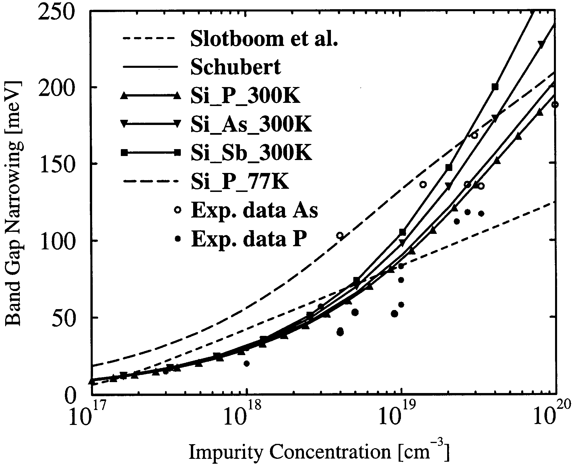
Many papers were dedicated to band gap narrowing in semiconductors in the last 20 years (e.g.). Despite all of this, the optimal ratio between accuracy of the results on the one hand, and the simplicity of model implementation on the other, appears still not to be achieved. Commercial device simulators, such as ATLAS, DESSIS, and MEDICI , use the logarithmic fifit models for band gap narrowing in Si, which are simple to implement, but deliver unphysical values for defifinite doping levels. The models proposed by del Alamo , and Bennet and Wilson cannot be used for concentrations below 1018 cm−3 , because an unrealistic increase of BGN is obtained. The established model after Slotboom et al., and the model after Klaasen, deliver too low values for concentrations of 1019 cm−3 and above. The functional form of models for Si is used for models for other materials (e.g. III-V compounds) or the BGN effect is left completely ignored. Comparison of these models with the model from this work, and with experimental data for Si is shown in Fig. 1. The physical limit our model offers (0 meV in the case of undoped materials), the physically sound explanation of some existing effects it gives, the ability to treat various semiconductor materials and dopants and the simplicity of the model make it very applicable for device simulation purposes.
The temperature dependence of the BGN in Si is shown in Fig. 3. Neglecting the stronger BGN at 77 K, especially for doping levels about 1019 cm−3 , may result in an error of about 50%. Therefore, even larger errors might be introduced into the simulation results, with respect to the electrical device characteristics. In the case of III-V semiconductors our model delivers a comparatively weaker BGN temperature dependence. Similar observations were done in the case of p-GaAs in [12,13]. Thus, our BGN model is the fifirst theoretically derived model predicting different shifts for various dopant species and taking temperature into account.
Our model extends its validity also for compound semiconductors by material composition dependent relative DOS masses for electrons and holes, on the one hand, and permitivity, on the other hand. The values used for the semiconductor electron number are calculated in a similar way. In Fig. 4 we present the results for boron and gallium doped SiGe for different Ge contents. The decrease of the BGN with increase of the Ge fraction was already experimentally observed in [14,15]. Our theoretical approach explains this effect by the decreased valence band density of states and increase of the relative permitivity in the SiGe alloy.

Fig1
In the case of p-type GaAs we obtain good agreement with experimental data . The few available experimental data for n-type GaAs suggest sometimes lower (open triangles in Fig. 5) values for BGN and more often higher (fifilled triangles) than our model delivers. This appears to emphasize the importance of modeling BGN in III-V semiconductors, rather than leaving this effect unconsidered, which is the case with the most device simulators.
In summary, a new physically based analytical band gap narrowing model is presented. It accounts for different dopants and is extended to compound semiconductors. The agreement with experimental data which, when available, are still rather uncertain is shown. In comparison with other existing models used for device simulation, the superiority of our new model is underlined. Finally, the important impact on the HBT device performance is studied.
上一篇: 化合物半导体光伏组件参数提取方法
下一篇: 化合物半导体射频器件的数值分析