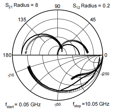
An overview of heterostructure RF device simulation for industrial application based on III-V compound semiconductors has been given in [1]. Here, we present the most recent achievements in numerical simulation for industrial heterostructure devices, together with relevant industrial applications (GaAs, InP, and SiGe HBTs).
To cope with explosive development costs and strong competition in the semiconductor industry today, Technology Computer-Aided Design (TCAD) methodologies are extensively used in development and production. Several questions during device fabrication, such as performance optimization and process control, can be addressed by simulation. The choice of a given simulation tool or a combination of tools depends to a large extent on the complexity of the particular task, on the desired accuracy of the problem solution, and on the available human, computer, and time resources.
Optimization of geometry, doping, materials, and material compositions targets high output power, high breakdown voltage, high speed (high fT and fmax), low leakage, low noise, and low power consumption. This is a challenging task that can be signifificantly supported by device simulation. While DC simulation is suffificient for optimization of breakdown voltages, turn-on voltages, or leakage currents, AC simulation is required for speed, noise, and power issues.
There are several challenges which are specifific for modeling and simulation of heterostructure devices. The characterization of the physical properties of III-V and SiGe compounds is required for wide ranges of material compositions, temperatures, doping concentrations, etc. The model parameters must be verifified against several independent HEMT and HBT technologies to obtain a concise set used for all simulations.

Fig1
For example, the database for novel materials, such as the GaN or the GaSb systems, which have entered the III-V world with impressive device results, is still relatively poor. Modeling of stress-induced changes of the physical properties of strained material layers and consideration of piezoelectrical effects is a subject of ongoing research. Heterointerface modeling is a key issue for devices which include abrupt junctions. Thermionic emission, fifield emission, and tunneling effects critically determine the current transport, especially in double heterojunction bipolar transistors (DHBTs).
Two-dimensional device simulation proved to be valuable for understanding the underlying device physics and for improving the device reliability . Bias-dependent Sparameters hold the full small-signal RF information about the device behavior and allow process control beyond the information about the DC quantities.
In addition, we set up a mixed-mode circuit to compare large-signal measurement data in the small-signal range. Fig. 2 gives simulated AC collector current iC versus AC input power PIN in good agreement with experimental data. Fig. 3 shows a comparison between measured and simulated AC output power POUT versus AC input power PIN. An almost perfect match of the curves is achieved in the small-signal area of the fifigure. A further increase of the input power causes harmonics in the device, which can not be obtained by the linear small-signal mode. Several methods which account for harmonic generation in the device, e.g. the harmonic balance method, have been evaluated in [28]. A software platform that integrates harmonic balance RF simulation technologies into an analogue/mixed signal design flflow framework is offered by Agilent.
下一篇: 化合物半导体纳米粒子的表面键合效应