We discuss the potential benefifits of using compound semiconductors for the detection of X- and g-ray radiation. While Si and Ge have become detection standards for energy dispersive spectroscopy in the laboratory, their use for an increasing range of applications is becoming marginalized by one or more of their physical limitations; namely the need for ancillary cooling systems or bulky cryogenics, their modest stopping powers and radiation intolerance. Compound semiconductors encompass such a wide range of physical properties that it is technically feasible to engineer a material to any application. Wide band-gap compounds offer the ability to operate in a wide range of thermal and radiation environments, whilst still maintaining sub-keV spectral resolution at hard X-ray wavelengths. Narrow band-gap materials, on the other hand, offer the potential of exceeding the spectral resolution of both Si and Ge, by as much as a factor of 3. Assuming that the total system noise can be reduced to a level commensurate with Fano noise, spectroscopic detectors could work in the XUV, effectively bridging the gap between the ultraviolet and soft X-ray wavebands. Thus, in principle, compound semiconductor detectors can provide continuous spectroscopic coverage from the far infrared through to g-ray wavelengths. However, while they are routinely used at infrared and optical wavelengths, in other bands, their development has been plagued by material and fabrication problems. This is particularly true at hard X-ray and g-ray wavelengths, where only a few compounds (e.g., GaAs, CdZnTe and HgI2) have evolved suffificiently to produce working detection systems. In this paper, we examine the current status of research in compound semiconductors and by a careful examination of material properties and future requirements, recommend a number of compounds for further development. In the longer term, when material problems are suffificiently under control, we believe the future lies in the development of heterostructures and inserted interface layers to overcome contacting problems and quantum heterostructures and superlattices to facilitate low-noise readout.
The term compound semiconductor encompasses a wide range of materials, most of which crystallize in either the zincblende (ZB), wurtzite or rocksalt crystal structures. They were fifirst investigated as radiation detectors in 1945 by Van Heerden , who demonstrated that silver chloride crystals when cooled to low temperatures were capable of detecting g-rays, a-particles and bparticles. This work was later extended to the thallious halides by Hofstadter in 1949. Strangely, at this time, the elemental semiconductors were not anticipated to be responsive to radiation and it was not until several months later than McKay managed to measure the polonium a-ray spectrum using a Ge surface barrier detector. While the subsequent development of Ge and Si radiation detectors was rapid, largely due to the explosive rise of the semiconductor industry, mixed-element and compound semiconductors, such as the alkali-metal halides, CdTe, CdZnTe and HgI2, were plagued by material problems caused by severe micro-crystallinity, high defect densities, impurities and stoichiometric imbalances. Until the 1960s very little additional work was carried out and the reader is referred to the survey of Prince and Polishuk . Since this time, progress has been incremental, but hardly spectacular and the reader is referred to the more recent review of McGregor and Harmon.
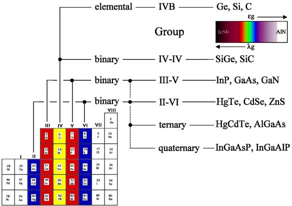
Compound semiconductors are generally derived from elements in groups II to VI of the periodic table. They are so useful because of the shear range of compounds available, compared to the elemental semiconductors, Sn-a, C, Si and Ge. Most elements in these groups are soluble within each other, forming homogeneous solid solutions. These solutions occur when atoms of a particular element are able to substitute a given constituent of a different material without altering its crystal structure. In order that atoms can form solid solutions over large ranges of miscibility, they should satisfy the Hume– Rothery rules, namely that.

Fig1
Group I–VII compounds can also form semiconductors, which exhibit a very large ionicity and energy gaps considerably larger than many III–V compounds: The latter is a direct consequence of the fact that bonding in these materials is almost entirely ionic and not covalent as in VI–VI, III–IV and most II–VI materials. Specifific examples include the silver halides, AgCl and AgBr, which were some of the fifirst compound semiconductors demonstrated to be sensitive to ionizing radiation.
From the above categories we can make several generalizations. For example, we note a clear tendency for the band-gap energy and melting point to increase with increasing ionicity (i.e., going from group IV to III–V through to II–VI and fifinally to group I–VII compounds), while micro-hardness decreases. There is also a clear tendency for the band-gap energy to decrease with increasing lattice constant by roughly a factor of 2 ( A. This is true for all groups, except group I–VII materials, which show little variation.
上一篇: 化合物半导体衬底加工的进展