Compound semiconductor materials such as GaAs and InP have distinct advantages over the more traditional silicon, chief of which is the greater electron mobility within the substrate, allowing greater use in low-noise, high gain applications. However, the advantages of these materials come with corresponding disadvantages. As these materials become attractive for high power applications, they become less suited for one of the major byproducts of this application – heat. In contrast to silicon, these materials have a much lower thermal conductivity, which leads to the primary method of heat management – wafer thinning.
In order to manage the heat, these materials will first be thinned (to minimize the overall thermal resistance), and then patterned with backside metallized vias, which serve both as heat sinks, and as a grounding back plane for the circuitry of the device.
This paper discusses recent advances in production technologies intended to address the challenges presented by this process, and allow for high yield manufacturing. First, the challenge of handling these fragile thinned substrates for the required post thinning processes of lithography, etch, and metallization will be discussed. Then, advances in lithography technologies for the alignment and patterning of the vias will be explored. Finally, new processes for compound semi technologies – spray coating and plasma assisted direct wafer bonding – will be presented.
In the past, this process would use wax. The benefit was that, by elevating the temperature, the overall adhesion of the wax would decrease drastically, allowing removal of the substrates with very little applied force. Challenges with this method are that, once the substrate has been removed, the residual wax would need to be removed via a solvent cleaning process, which is quite hazardous to the thinned and fragile substrate. In addition, removal of the substrate was frequently performed by human hand, again leading to yield losses.
A new system has been developed which, although it can be designed to process waxes, finds its full advantage using a different adhesion technology - that of double sided thermal release tapes (Figure 1). The system integrates all steps used to perform the mounting of the compound semiconductor wafer onto the carrier. In order to accomplish this, the system will simultaneously process both the carrier substrate and the device substrate through separate steps, with the final result being the bonded pair, suitable for thinning and further processing.

Fig1
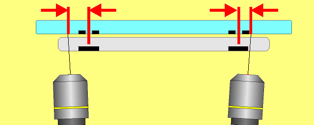
During the digitization process of mask alignment keys, the mask itself is placed into direct contact with the wafer chuck, and the focus of the microscopes is established in that plane. Then, when the mask is lifted, and the wafer inserted in its place (face down - appropriate for backside patterning), the patterns on the face of the wafer, since they are also in contact with the chuck, are also in focus, with no movement of the microscopes.
This is where the problem occurs with carrier-mounted substrates – the carrier prevents contact between the patterns of device wafer and wafer chuck. In the past, a workaround to this process was developed. In this case, a dummy substrate, representing the thickness of the sapphire, would be inserted under the mask. When the optics are focused onto the mask, the focal plane is re-calibrated to account for the thickness of the carrier.
上一篇: 化合物半导体表面金属纳米粒子的形成与性质
下一篇: 化合物半导体辐射探测器