First and foremost, I would like to express my heartfelt thanks to my thesis advisor Professor Rachel S. Goldman for guidance and patience throughout my doctoral research. I learned three precious lessons from her as follows. First, any theoretical prediction should be experimentally proved. Second, we must be open to new ideas and ready to modify our opinions if contradictory evidence emerges. Third, everything should be based on intellectual honesty. These simple yet profound principles which she taught me resulted in this dissertation. I believe that her enthusiasm and high standard for work will benefit me in the future.
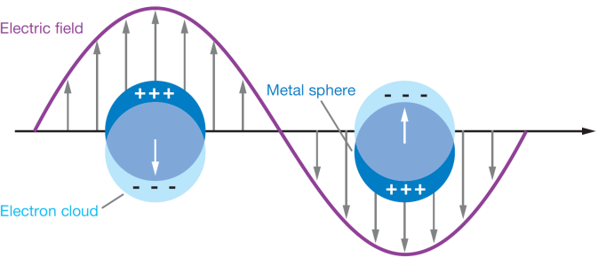
Surface plasmon resonance (SPR) is the collective oscillation of electrons in a solid or liquid induced by incident light.1 The resonance occurs when the frequency of incident light matches the natural frequency of electrons oscillating against the restoring force of positive nuclei, as shown in Fig. 1.1 Typical plasmonic materials are metals because of high free electron density. Recently, SPR of metallic NPs on semiconductor surfaces have shown significant promise for various applications including enhanced light emission, efficient solar energy harvesting, high sensitivity biosensing, and negative refractive index metamaterials. It has been shown that metallic NPs enable the generation of SPR in the ultraviolet, visible, and infrared ranges, where SPR energies are inversely proportional to diameters of the metallic NPs, as shown in Fig. 1.2.
Existing methods for the fabrication of these metallic NPs require complex multi-level processing such as lithography. Meanwhile, ion irradiation-induced surface NP formation involves the self-assembly process for achieving dense arrays of metallic NPs on semiconductor surfaces. In this thesis, we explore a new plasmonic material (Ga) fabricated via FIB irradiation for enhancing energy conversion efficiencies of semiconductors. Here, we report formation and properties of FIB-induced metallic NPs on compound semiconductor surfaces.
In particular, this thesis focuses on the influence of metallic NP on optical properties of semiconductors, and therefore, it is important to discuss how SPR of metallic NPs is related to the light emission efficiency of semiconductor surfaces. Figure 1.4(a) shows a typical PL spectra taken from GaAs layers grown on a GaAs substrate in Goldman group Gen-II molecular beam epitaxy system. To enhance the PL efficiency of semiconductors such as GaAs layers, SPR of metallic NPs have been utilized to tailor light-matter interaction in metal-semiconductor composites.1,13,17 The metallic NP-enhanced light emission efficiency of semiconductor surfaces has been explained mainly in terms of enhanced spontaneous emission rate.13 Meanwhile, the influence of surface metallic NPs on the incident light absorption efficiency of semiconductor layers has been a remaining issue for the metallic NP SPR-enhanced light emission efficiency of semiconductor surfaces. Figure 1.4(b) and 1.4(c) shows a band diagram and a schematic illustration where the relative influences of metallic NP SPR on absorption and emission processes in semiconductor layers are considered. One of this thesis study’s goals is studying the influence of Ga NP diameter-dependent SPR on both absorption and emission processes.

Fig1.1
All FIB irradiation described in this thesis was carried out in a FEI NOVA 200 dual beam workstation shown schematically in Fig. 2.1. The FIB system consists of an ion beam column, an electron beam column, an energy dispersive x-ray, and secondary electron detectors, in a high vacuum chamber with 10-5 torr base pressure. This system combines a high-resolution secondary electron microscope for surface imaging, a Ga+ FIB for irradiation and patterning, and x-ray microanalysis for characterization. During FIB irradiation, surface imaging and x-ray microanalysis are achieved via the collection of secondary electrons and characteristic x-rays, respectively.
上一篇: 化合物半导体表面的电子控制化学稳定性
下一篇: 化合物半导体衬底加工的进展