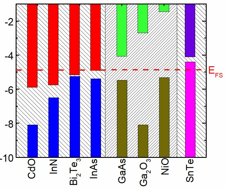
Effects of humid environment on the degradation of semiconductors were studied to understand the role of the surface charge on material stability. Two distinctly different semiconductors with the Fermi level stabilization energy EFS located inside the conduction (CdO) and valence band (SnTe) were selected and effects of an exposure to 85℃ and 85% relative humidity conditions on their electrical properties were investigated. Undoped CdO films with bulk Fermi level EF below EFS and positively charged surface are very unstable. The stability greatly improves with doping when EF shifts above EFS and the surface becomes negatively charged. This charge-controlled reactivity is further confirmed by the superior stability of undoped p-type SnTe with EF above EFS. These distinct reactivities are explained by the surface attracting either the reactive OH- or passivating H+ ions. The present results have important implications for understanding the interaction of semiconductor surfaces with water or in general with ionic solutions.
The progressing miniaturization and increasing surface to volume ratio in modern semiconductor devices greatly emphasizes the importance of the semiconductor surface stability under various environmental conditions. In addition, in some instances, e.g., sensors or water splitting devices, the surface plays a role essential in the device operation and cannot be separated from the ambient. Therefore, there is a need to fully understand the factors affecting chemical reactions on semiconductor surfaces induced by different environments.
Different factors have been identified to impact the stability of compound semiconductors upon moisture exposure. The nature and the strength of the chemical bonds are one of the main factors that determine the material stability and the degradation process. It is well known that a prolonged exposure of weakly bound perovskite-type hybrid materials to moisture results in the material decomposition1,2 . Also, Hisaka et. al3 found that the degradation of AlGaAs/InGaAs pseudomorphic high-electron-mobility transistors started with the oxidization reaction at the drain side corner under high humidity conditions. Comizzoli et. al.4 found that the performance degradation of their avalanche photodiodes upon moisture exposure began with the corrosion of the SiN passivation layer.
Numerous studies have shown that surface Fermi energies of semiconductor materials are pinned at the Fermi stabilization energy which is a common energy EFS reference located at about 4.9 eV below the vacuum level. Although in most semiconductors is located inside the band gap, in some instances EFS the can fall into either the conduction or the valence band, as shown in Figure 1. In these extreme cases, the semiconductors EFS show a clear proclivity for the n-type or ptype doping. The surface Fermi energy is pinned by dangling-bond-like defects whose nature.

Fig1
Consequently, the surface electrical charge can be controlled by a judicious choice of the material, doping type and the doping level. Thus a surface of undoped CdO with located deeply in conduction band12 is positively charged whereas the surface of undoped SnTe with located in the valence band16 is negatively charged. The surface charge can also be controlled by shifting of the Fermi energy with an intentional doping.
上一篇: 化合物半导体纳米线光电探测器
下一篇: 化合物半导体表面金属纳米粒子的形成与性质