Light detection by semiconductor nanowires (NWs) is an active area of research. The interest in NW photodetector devices was originally motivated by the fascinating properties of NW materials and structures, which offer new ways to improve the detector performance as well as to integrate multiple functionalities. Indeed, NWs exhibit unique photonic and electrical properties stemming from their anisotropic geometry, high surface-tovolume ratio, small footprint, and crystalline perfection. Even above the quantum confinement size regime, NW photoconductors can yield higher light sensitivity than their bulk counterparts due to the large surface-to-volume ratio and small dimensions. The waveguiding properties of individual NWs as well as the antireflection and light trapping properties of NW arrays are also beneficial for light detection since efficient absorption can be achieved within a small volume of active material. Availability of compound semiconductor materials and functional NW heterostructures, either axial or radial, has enabled bandgap engineering and translation of conventional photodetector device concepts into NW architectures. In addition, NWs can be integrated with CMOS technology either by direct growth of high-quality nanocrystals on Si or by different transfer schemes such as dielectrophoresis or dry printing. Integration of NW detectors and light emitters into functional platforms for optical interconnects, quantum photonics and biosensors is currently an area of intense activity and growing interest in both electronics and photonics research communities.
Thanks to the ongoing advancement in the growth and fabrication methodologies, NWs of almost all the existing semiconductor materials can be now realized by means of either top-down or bottom-up approaches. The advantage of the bottom-up NW synthesis is the possibility to reduce the object dimensions disregarding the limitations imposed by the lithographic techniques while preserving lateral surface flatness. A high degree of control over the composition, doping, and morphology is achieved today with a bottom-up approach. It has also become possible to integrate different functionalities in NWs, using doping and homo- or heterojunctions of compound semiconductor materials, in order to engineer their properties at the nanoscale.
Photoconductivity is a well-known property of semiconductors that change their electrical conductivity under illumination (Bube, 1960). Photoconductive semiconductors have broad application in light detection and photovoltaic energy conversion. The observation of high photoresponsivity in semiconductor NWs and recent advances in the understanding of the photoconduction mechanism in low-dimensional systems with a high density of surface states is attracting growing interest for the potential use of NWs as photosensing elements in highly integrated optoelectronic devices, optical interconnects, transceivers, etc. The basic concepts specifically related to photoconductivity in NWs are presented in the following.
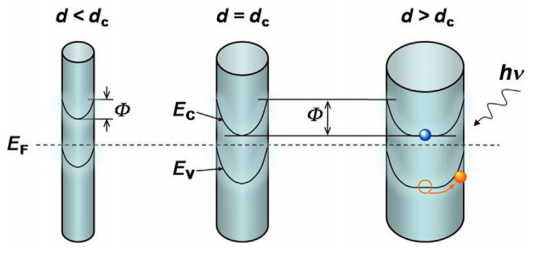
where v¼μF is the carrier drift velocity and S is the nondepleted crosssection surface of the NW. Due to the pinning of the Fermi energy at the NW lateral surface, NWs exhibit a depletion space-charge layer and the conducting surface S is in general smaller than the physical NW cross section. Band bending at the surface provides physical separation of electrons and holes and can lead to a significantly enhanced photocarrier lifetime (persistent photoconductivity). A schematic of surface state effects on band bending and photogenerated carrier separation in n-type NWs with different diameters is depicted in Fig. 1.

Fig1
Overall, semiconductor NWs show high photoconductive gain due to a combination of the following: (1) the photocarrier lifetime is considerably prolonged due to charge separation promoted by surface states, (2) the carrier transit time is significantly reduced due to the high mobility achievable in high-quality, defect-free single crystal NWs combined with small interelectrode distances, and (3) the conducting surface changes due to the modulation of the depletion region. Numerous experimental studies of the NW photoconductivity have indeed reported a high sensitivity to light and a very high photoconductive gain.
Light absorption in NW materials is subject to specific effects stemming from the NW geometry and the low dimensionality, such as optical birefringence, light scattering, and waveguiding effects (light funneling), which will now be discussed in more detail.
The optical properties of vertical arrays of InP, Si, GaAs, and GaP NWs have been investigated experimentally (Muskens et al., 2008). It was found that, for typical NW diameters around 50 nm, diffuse multiple light scattering dominates the optical properties of the NW arrays and that depending on the ratio between the absorption and scattering mean free path (the latter can be controlled by varying the NW diameter or by infiltration with refractive index matching materials), absorption losses can be strongly suppressed in the NW arrays. This has obvious implications for the design of efficient NW absorbers in NW-based photovoltaic cells, or in determining the spectral response of NW photodetectors.
上一篇: 化合物半导体纳米粒子的表面键合效应
下一篇: 化合物半导体表面的电子控制化学稳定性