The need for polishing silicon wafer is to obtain a smooth surface for sprucing the semiconductor devices on the wafer surface. Therefore the wafer surface should be extremely flat, mirror like and particle free. Currently chemical mechanical polishing (CMP) is used in the polishing industry to polish silicon wafer. In CMP the chemical action weakens the atomic bonding of the wafer surface and the rotatory mechanical action assist the material removal. In the present work chemical etching of Si (100) with potassium hydroxide (KOH) and polishing with Double Disk Magnetic Abrasive Finishing (DDMAF) is proposed. Comparison is made for surface roughness while polishing Si (100) with DDMAF at different combination of polishing speed, working gap and mesh no. of alumina abrasive. The communication further extends a comparative study on surface morphology with scanning electron microscopy (SEM) and atomic force microscopy (AFM) for unpolished sample and polished sample obtained at best combination of process parameters .
Gui et al. studied the CMP applications in Direct Wafer Bonding (DWB) which was used to develop and fabricate novel sensors and actuators. DWB is a bonding process carried out at low temperature to join exotic material such as glass, quartz; sapphires etc. with smooth enough surface less than one nanometers. The study was focused to analyze and compare the influence of surface morphology in DWB and different wafer smoothening processes.
Kang et al. studied the effect of pH value of the slurry on poly silicon chemical mechanical polishing. They found that poly silicon wafer polishing was the function of pH value of the slurry in abrasive free and silica based slurries. The measurements of dynamic etch rate and MRR as a function of pH along with friction force and pad temperatures were made. They concluded that polysilicon CMP process was strongly influenced by mechanical factor; however bare silicon wafer polishing was dominated by chemical effect. The result showed that in abrasive free slurries, the dynamic etch rate and friction force did not show any change in the presence of native oxide on poly and bare silicon.
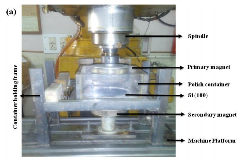
The DDMAF experimental frame work is shown in Fig 1(a) was used to perform the experiments. The schematic diagram of the same is shown in Fig 1(b). The frame work consisted of primary magnet and secondary magnet. The primary magnet was mounted on the spindle of a vertical CNC Beaver milling machine. The secondary magnet was rested on the platform of the machine. The working gap between silicon workpiece and primary magnet was filled with MAPs to form FMAB for executing the polishing action in the presence of magnetic field. The working gap was varied between 5mm to 6mm subject to the condition that the magnetic field in the polishing zone existed between 0.40 Tesla to 0.38 Tesla. The working gap of secondary magnet was fixed at a distance of 5 mm from the workpiece.

Fig1(a)
From Fig.2 (b) it can be observed that as the working gap increases the surface roughness of polished Si (100) also increases. This may be due to the fact that, as the working gap increases the number of magnetic line of forces passing through the workpiece decreases. The decrease in magnetic lines of forces reduces the FMAB strength and therefore surface roughness increases. The variation of mesh no. of alumina abrasive with surface roughness can be inferred from Fig. 2(c). The trend shows that with an increase in the mesh no. of alumina abrasives the surface roughness of polished wafer decreases. This may be due the reason that an increase in mesh number increases cutting edges in the polishing zone which removes the peaks from the work material and the surface roughness of polished silicon wafer decreases.
下一篇: 光伏多晶硅晶界杂质吸收与钝化的层次结构